General-purpose I/Os (GPIO) RM0444
238/1390 RM0444 Rev 5
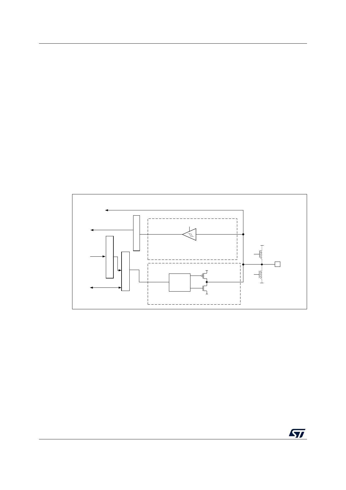
7.3.10 Output configuration
When the I/O port is programmed as output:
• The output buffer is enabled:
– Open drain mode: A “0” in the Output register activates the N-MOS whereas a “1”
in the Output register leaves the port in Hi-Z (the P-MOS is never activated)
– Push-pull mode: A “0” in the Output register activates the N-MOS whereas a “1” in
the Output register activates the P-MOS
• The Schmitt trigger input is activated
• The pull-up and pull-down resistors are activated depending on the value in the
GPIOx_PUPDR register
• The data present on the I/O pin are sampled into the input data register every AHB
clock cycle
• A read access to the input data register gets the I/O state
• A read access to the output data register gets the last written value
Figure 19 shows the output configuration of the I/O port bit.
Figure 19. Output configuration
7.3.11 Alternate function configuration
When the I/O port is programmed as alternate function:
• The output buffer can be configured in open-drain or push-pull mode
• The output buffer is driven by the signals coming from the peripheral (transmitter
enable and data)
• The Schmitt trigger input is activated
• The weak pull-up and pull-down resistors are activated or not depending on the value
in the GPIOx_PUPDR register
• The data present on the I/O pin are sampled into the input data register every AHB
clock cycle
• A read access to the input data register gets the I/O state
Figure 20 shows the Alternate function configuration of the I/O port bit.
MSv33184V3
Output
control
Output data register
Bit set/reset registers
Input data register
Read
To / from on-chip
peripherals,
power control
and EXTI
Analog input/output
P-MOS
Output driver
V
DDIOx
V
SS
N-MOS
Push-pull or
open-drain
V
SS
V
DDIOx
on/off
on/off
I/O pin
TTL Schmitt trigger
On
Write
Read/write
Pull
up
Pull
down
Input driver

 Loading...


