RM0444 Rev 5 377/1390
RM0444 Analog-to-digital converter (ADC)
403
Main features
• Supported temperature range: –40 to 125 °C
• Linearity: ±2 °C max., precision depending on calibration
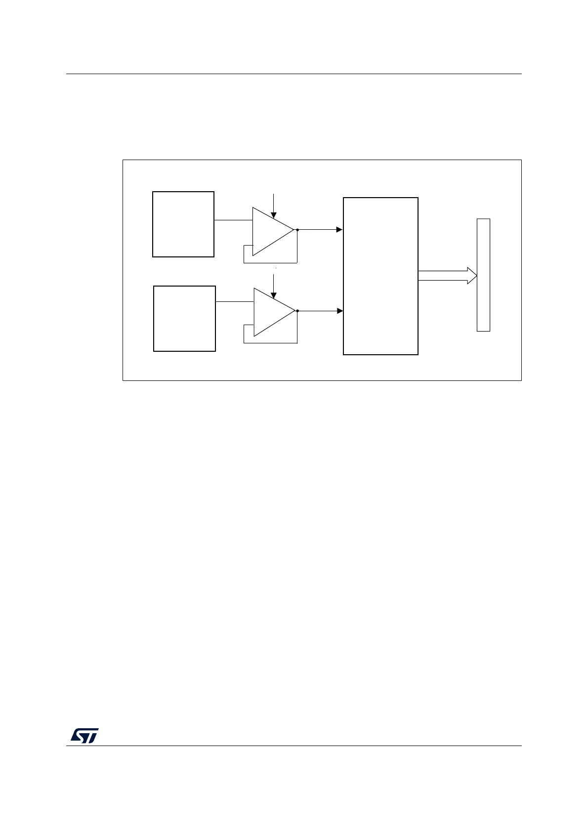
Figure 57. Temperature sensor and V
REFINT
channel block diagram
Reading the temperature
1. Select the ADC V
IN
[12] input channel
2. Select an appropriate sampling time specified in the device datasheet (T
S_temp
).
3. Set the TSEN bit in the ADC_CCR register to wake up the temperature sensor from
power down mode and wait for its stabilization time (t
START
).
4. Start the ADC conversion by setting the ADSTART bit in the ADC_CR register (or by
external trigger)
5. Read the resulting V
SENSE
data in the ADC_DR register
6. Calculate the temperature using the following formula
Where:
• TS_CAL2 is the temperature sensor calibration value acquired at TS_CAL2_TEMP
(refer to the datasheet for TS_CAL2 value)
• TS_CAL1 is the temperature sensor calibration value acquired at TS_CAL1_TEMP
(refer to the datasheet for TS_CAL1 value)
• TS_DATA is the actual temperature sensor output value converted by ADC
Refer to the specific device datasheet for more information about TS_CAL1 and
TS_CAL2 calibration points.
Note: The sensor has a startup time after waking from power down mode before it can output
V
SENSE
at the correct level. The ADC also has a startup time after power-on, so to minimize
the delay, the ADEN and TSEN bits should be set at the same time.
MSv62466V1
V
SENSE
TSEN control bit
Address/data bus
converted data
ADC V
IN
[13]
Temperature
sensor
Internal power
block
ADC
VREFEN control bit
ADC V
IN
[12]
+
-
+
-
V
REFINT
Temperature in °C()
TS_CAL2_TEMP TS_CAL1_TEMP–
TS_CAL2 TS_CAL1–
----------------------------------------------------------------------------------------------------
TS_DATA TS_CAL1–()TS_CAL1_TEMP+×=

 Loading...


