Digital-to-analog converter (DAC) RM0444
408/1390 RM0444 Rev 5
16.4.3 DAC channel enable
Each DAC channel can be powered on by setting its corresponding ENx bit in the DAC_CR
register. The DAC channel is then enabled after a t
WAKEUP
startup time.
Note: The ENx bit enables the analog DAC channelx only. The DAC channelx digital interface is
enabled even if the ENx bit is reset.
16.4.4 DAC data format
Depending on the selected configuration mode, the data have to be written into the specified
register as described below:
• Single DAC channel
There are three possibilities:
– 8-bit right alignment: the software has to load data into the DAC_DHR8Rx[7:0] bits
(stored into the DHRx[11:4] bits)
– 12-bit left alignment: the software has to load data into the DAC_DHR12Lx [15:4]
bits (stored into the DHRx[11:0] bits)
– 12-bit right alignment: the software has to load data into the DAC_DHR12Rx [11:0]
bits (stored into the DHRx[11:0] bits)
Depending on the loaded DAC_DHRyyyx register, the data written by the user is shifted and
stored into the corresponding DHRx (data holding registerx, which are internal non-memory-
mapped registers). The DHRx register is then loaded into the DORx register either
automatically, by software trigger or by an external event trigger.
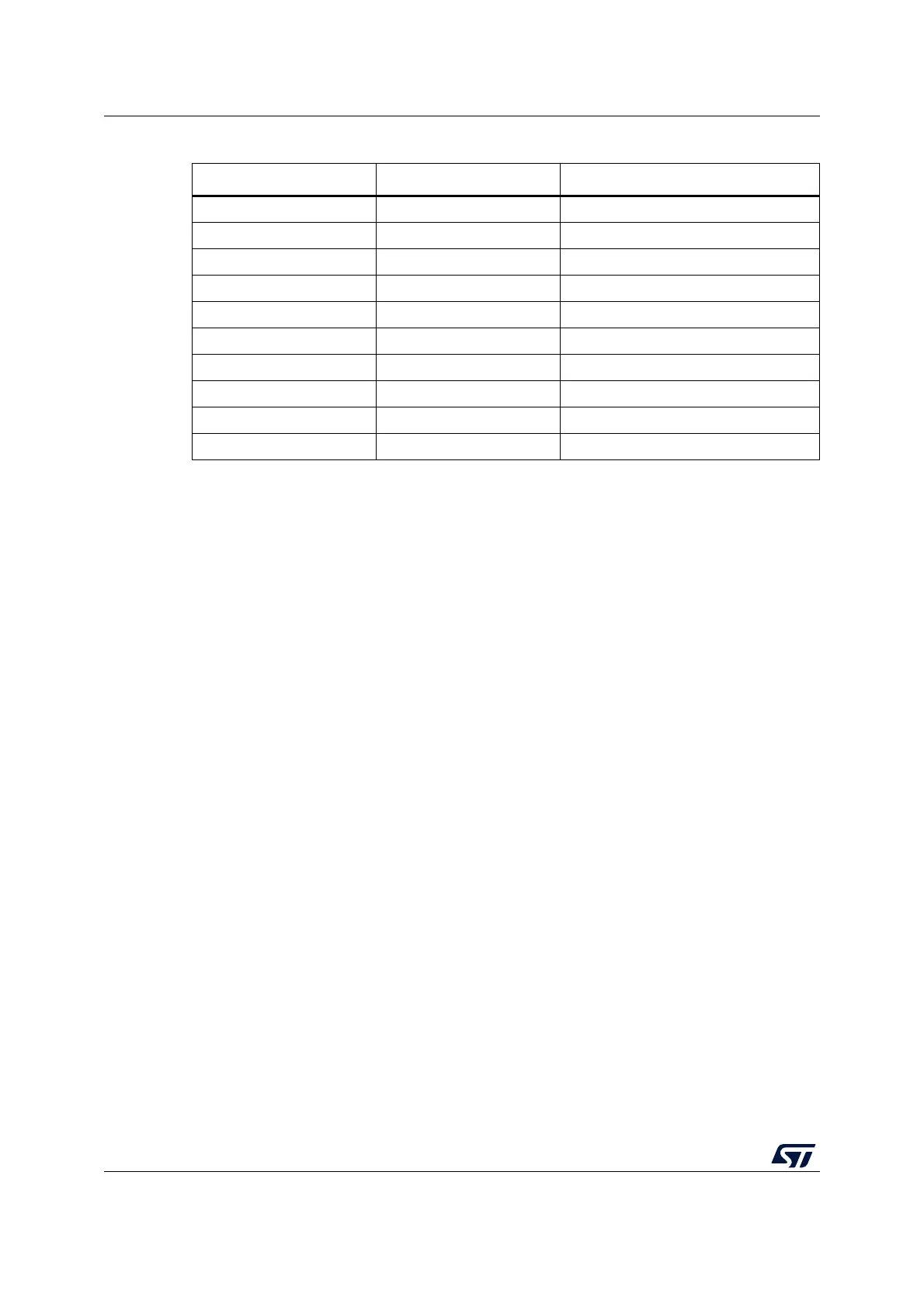
Table 82. DAC interconnection
Signal name Source Type
dac_hold_ck ck_lsi (selected in the RCC) LSI clock selected in the RCC
dac_chx_trg1 (x = 1, 2) tim1_trgo Internal signal from on-chip timers
dac_chx_trg2 (x = 1, 2) tim2_trgo Internal signal from on-chip timers
dac_chx_trg3 (x = 1, 2) tim3_trgo Internal signal from on-chip timers
dac_chx_trg5 (x = 1, 2) tim6_trgo Internal signal from on-chip timers
dac_chx_trg6 (x = 1, 2) tim7_trgo Internal signal from on-chip timers
dac_chx_trg8 (x = 1, 2) tim15_trgo Internal signal from on-chip timers
dac_chx_trg11 (x = 1, 2) lptim1_out Internal signal from on-chip timers
dac_chx_trg12 (x = 1, 2) lptim2_out Internal signal from on-chip timers
dac_chx_trg13 (x = 1, 2) exti9 External pin

 Loading...


