Power control (PWR) RM0444
156/1390 RM0444 Rev 5
4.4.17 Power Port E pull-down control register (PWR_PDCRE)
Address offset: 0x44
Reset value: 0x0000 0000. This register is not reset when exiting Standby modes and with
PWRRST bit in the APB peripheral reset register 1 (RCC_APBRSTR1).
Access: Additional APB cycles are needed to access this register vs. a standard APB
access (3 for a write and 2 for a read).
4.4.18 Power Port F pull-up control register (PWR_PUCRF)
Address offset: 0x48
Reset value: 0x0000 0000. This register is not reset when exiting Standby modes and with
PWRRST bit in the APB peripheral reset register 1 (RCC_APBRSTR1).
Access: Additional APB cycles are needed to access this register vs. a standard APB
access (3 for a write and 2 for a read).
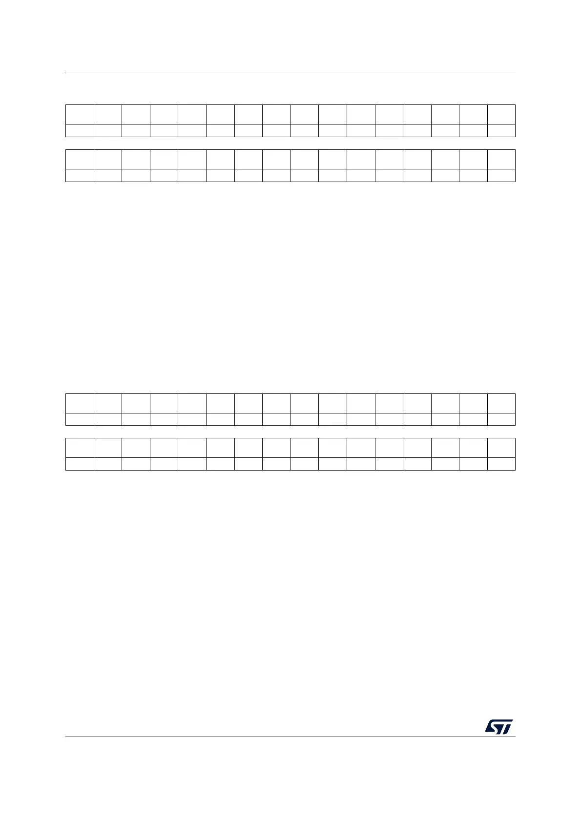
31 30 29 28 27 26 25 24 23 22 21 20 19 18 17 16
Res. Res. Res. Res. Res. Res. Res. Res. Res. Res. Res. Res. Res. Res. Res. Res.
1514131211109876543210
PU15 PU14 PU13 PU12 PU11 PU10 PU9 PU8 PU7 PU6 PU5 PU4 PU3 PU2 PU1 PU0
rw rw rw rw rw rw rw rw rw rw rw rw rw rw rw rw
Bits 31:16 Reserved, must be kept at reset value.
Bits 15:0 PUy: Port E pull-up bit y (y = 0 to 15)
(1)
Setting PUy bit while the corresponding PDy bit is zero and the APC bit of the PWR_CR3
register is set activates a pull-up device on the PE[y] I/O.
1. Only applies to STM32G0B1xx and STM32G0C1xx devices. Reserved for the other devices.
31 30 29 28 27 26 25 24 23 22 21 20 19 18 17 16
Res. Res. Res. Res. Res. Res. Res. Res. Res. Res. Res. Res. Res. Res. Res. Res.
1514131211109876543210
PD15 PD14 PD13 PD12 PD11 PD10 PD9 PD8 PD7 PD6 PD5 PD4 PD3 PD2 PD1 PD0
rw rw rw rw rw rw rw rw rw rw rw rw rw rw rw rw
Bits 31:16 Reserved, must be kept at reset value.
Bits 15:0 PDy: Port E pull-down bit y (y = 0 to 15)
(1)
Setting PDy bit while the APC bit of the PWR_CR3 register is set activates a pull-down
device on the PE[y] I/O.
1. Only applies to STM32G0B1xx and STM32G0C1xx devices. Reserved for the other devices.

 Loading...


