RM0444 Rev 5 295/1390
RM0444 Direct memory access controller (DMA)
297
10.6.7 DMA register map
The table below gives the DMA register map and reset values.
Bits 31:0 MA[31:0]: peripheral address
It contains the base address of the memory from/to which the data will be read/written.
When MSIZE[1:0] = 01 (16 bits), bit 0 of MA[31:0] is ignored. Access is automatically aligned
to a half-word address.
When MSIZE = 10 (32 bits), bits 1 and 0 of MA[31:0] are ignored. Access is automatically
aligned to a word address.
In memory-to-memory mode, this register identifies the memory source address if DIR = 1
and the memory destination address if DIR = 0.
In peripheral-to-peripheral mode, this register identifies the peripheral source address
DIR = 1 and the peripheral destination address if DIR = 0.
Note: this register is set and cleared by software.
It must not be written when the channel is enabled (EN = 1).
It is not read-only when the channel is enabled (EN = 1).
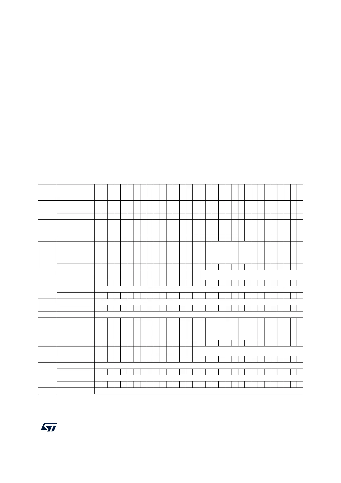
Table 50. DMA register map and reset values
Offset Register
31
30
29
28
27
26
25
24
23
22
21
20
19
18
17
16
15
14
13
12
11
10
9
8
7
6
5
4
3
2
1
0
0x000
DMA_ISR
Res.
Res.
Res.
Res.
TEIF7
HTIF7
TCIF7
GIF7
TEIF6
HTIF6
TCIF6
GIF6
TEIF5
HTIF5
TCIF5
GIF5
TEIF4
HTIF4
TCIF4
GIF4
TEIF3
HTIF3
TCIF3
GIF3
TEIF2
HTIF2
TCIF2
GIF2
TEIF1
HTIF1
TCIF1
GIF1
Reset value 0000000000000000000000000000
0x004
DMA_IFCR
Res.
Res.
Res.
Res.
CTEIF7
CHTIF7
CTCIF7
CGIF7
CTEIF6
CHTIF6
CTCIF6
CGIF6
CTEIF5
CHTIF5
CTCIF5
CGIF5
CTEIF4
CHTIF4
CTCIF4
CGIF4
CTEIF3
CHTIF3
CTCIF3
CGIF3
CTEIF2
CHTIF2
CTCIF2
CGIF2
CTEIF1
CHTIF1
CTCIF1
CGIF1
Reset value 0000000000000000000000000000
0x008
DMA_CCR1
Res.
Res.
Res.
Res.
Res.
Res.
Res.
Res.
Res.
Res.
Res.
Res.
Res.
Res.
Res.
Res.
Res.
MEM2MEM
PL[1:0]
MSIZE[1:0]
PSIZE[1:0]
MINC
PINC
CIRC
DIR
TEIE
HTIE
TCIE
EN
Reset value 000000000000000
0x00C
DMA_CNDTR1
Res.
Res.
Res.
Res.
Res.
Res.
Res.
Res.
Res.
Res.
Res.
Res.
Res.
Res.
Res.
Res.
NDTR[15:0]
Reset value 0000000000000000
0x010
DMA_CPAR1 PA[31:0]
Reset value 00000000000000000000000000000000
0x014
DMA_CMAR1 MA[31:0]
Reset value 00000000000000000000000000000000
0x018 Reserved Reserved.
0x01C
DMA_CCR2
Res.
Res.
Res.
Res.
Res.
Res.
Res.
Res.
Res.
Res.
Res.
Res.
Res.
Res.
Res.
Res.
Res.
MEM2MEM
PL[1:0]
MSIZE[1:0]
PSIZE[1:0]
MINC
PINC
CIRC
DIR
TEIE
HTIE
TCIE
EN
Reset value 000000000000000
0x020
DMA_CNDTR2
Res.
Res.
Res.
Res.
Res.
Res.
Res.
Res.
Res.
Res.
Res.
Res.
Res.
Res.
Res.
Res.
NDTR[15:0]
Reset value 0000000000000000
0x024
DMA_CPAR2 PA[31:0]
Reset value 00000000000000000000000000000000
0x028
DMA_CMAR2 MA[31:0]
Reset value 00000000000000000000000000000000
0x02C Reserved Reserved.

 Loading...


