Power control (PWR) RM0444
120/1390 RM0444 Rev 5
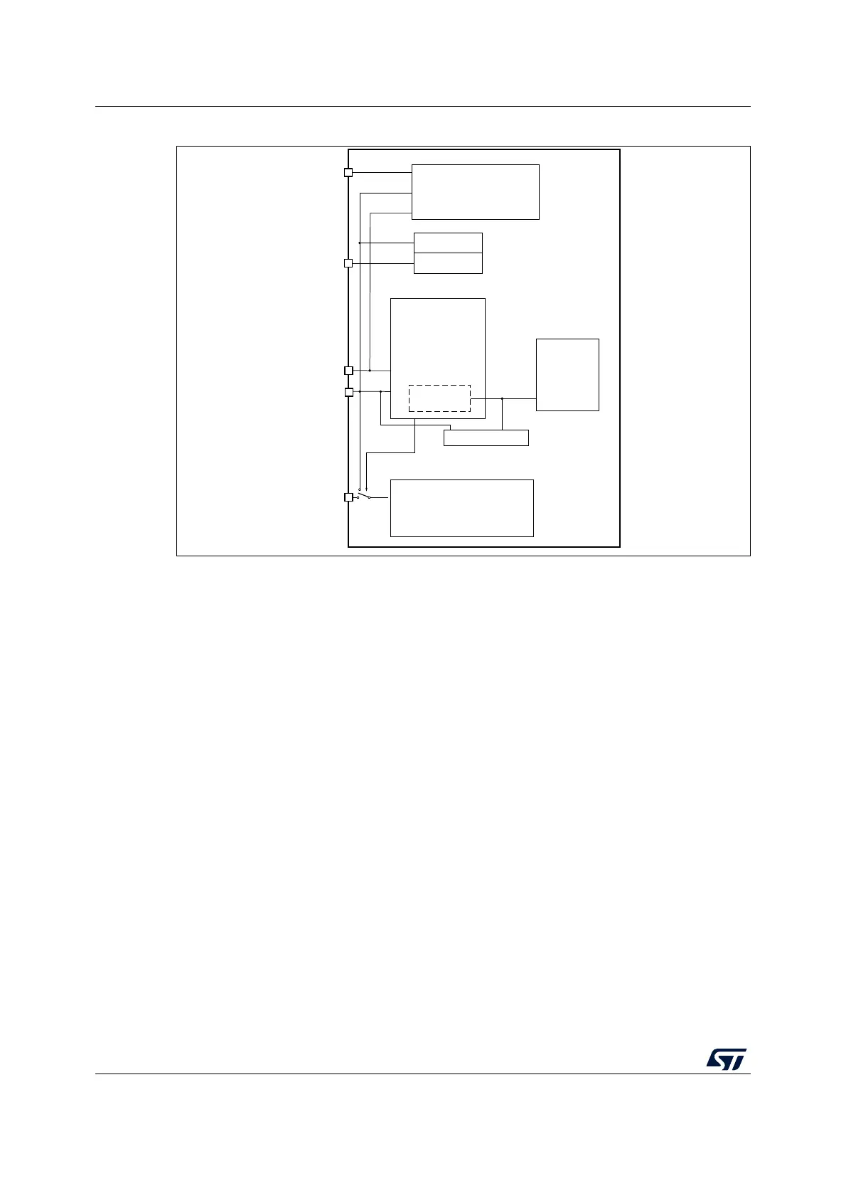
Figure 5. Power supply overview
4.1.1 ADC and DAC reference voltage
To ensure a better accuracy on low-voltage inputs and outputs, the user can connect to
V
REF+
a separate reference voltage lower than V
DDA
. V
REF+
is the highest voltage,
represented by the full scale value, for an analog input (ADC) or output (DAC) signal.
V
REF+
can be provided either by an external reference of by an internal buffered voltage
reference (VREFBUF).
The internal buffered voltage reference is enabled by setting the ENVR bit in the VREFBUF
control and status register (VREFBUF_CSR). The internal buffered voltage reference is set
to 2.5 V when the VRS bit is set and to 2.048 V when the VRS bit is cleared. The internal
buffered voltage reference can also provide the voltage to external components through
V
REF+
pin. Refer to the device datasheet and to Section 17: Voltage reference buffer
(VREFBUF) for further information.
4.1.2 Battery backup of RTC domain
To retain the content of the backup registers and supply the RTC and TAMP functions when
V
DD
is turned off, the VBAT
pin can be connected to an optional backup voltage supplied by
a battery or by another source.
The VBAT pin powers the RTC and TAMP units, the LSE oscillator and the PC13 to PC15
I/Os, allowing the RTC and TAMP to operate even when the main power supply is turned off.
The switch to the V
BAT
supply is controlled by the power-down reset embedded in the Reset
block.
MSv63104V1
V
DDA
domain
RTC domain
D/A converter
A/D converter
Standby circuitry
(Wakeup, IWDG)
Voltage
regulator
Core
SRAM
Digital
peripherals
Low-voltage
detector
LSE crystal 32.768 kHz osc
BKP registers
RCC BDCR register
RTC and TAMP
Comparators
Voltage reference buffer
I/O ring
V
CORE
domain
Temp. sensor
Reset block
PLL, HSI
Flash memory
V
DDIO1
VREF+
V
DD
domain
V
CORE
VSS/VSSA
VDD/VDDA
VBAT
V
DDA
V
REF+
V
SSA
V
SS
V
DD
V
DDIO1
domain
I/O ring
V
DDIO2
domain
VDDIO2
V
DDIO2

 Loading...


