Inter-integrated circuit (I2C) interface RM0444
930/1390 RM0444 Rev 5
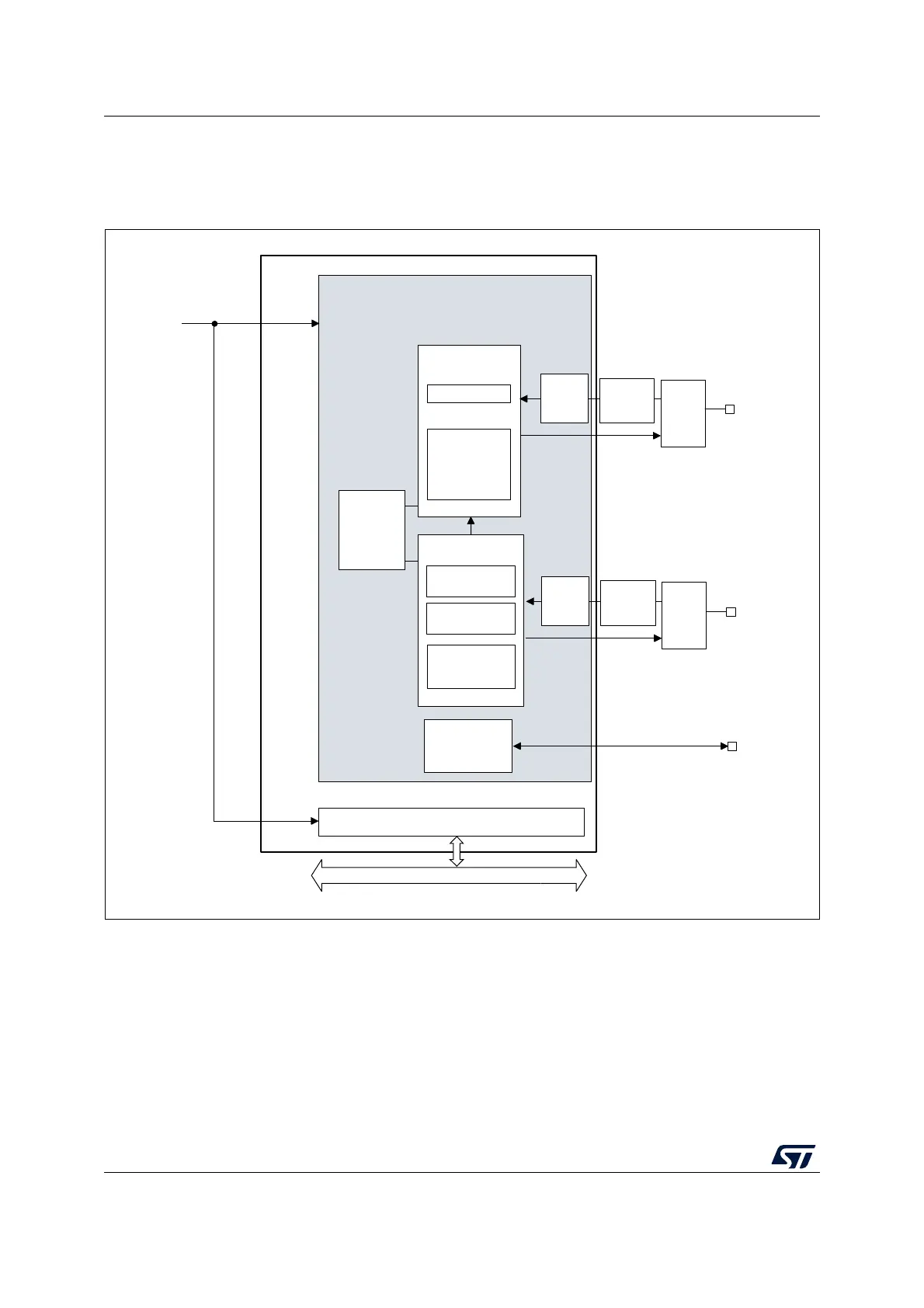
32.4.2 I2C2 block diagram
The block diagram of the I2C2 interface is shown in Figure 284.
Figure 284. I2C2 block diagram
For I2C I/Os supporting 20 mA output current drive for Fast-mode Plus operation, the driving
capability is enabled through control bits in the system configuration controller (SYSCFG).
Refer to Section 32.3: I2C implementation.
MSv46199V2
Wakeup
on
address
match
SMBUS
PEC
generation/
check
Shift register
Data control
SMBus
Timeout
check
Clock control
Master clock
generation
Slave clock
stretching
SMBus Alert
control &
status
Digital
noise
filter
I2C1_SCL
I2C1_SMBA
Registers
APB bus
GPIO
logic
Analog
noise
filter
Digital
noise
filter
I2C1_SDA
GPIO
logic
Analog
noise
filter
PCLK
I2CCLK

 Loading...


