Embedded Flash memory (FLASH) RM0444
106/1390 RM0444 Rev 5
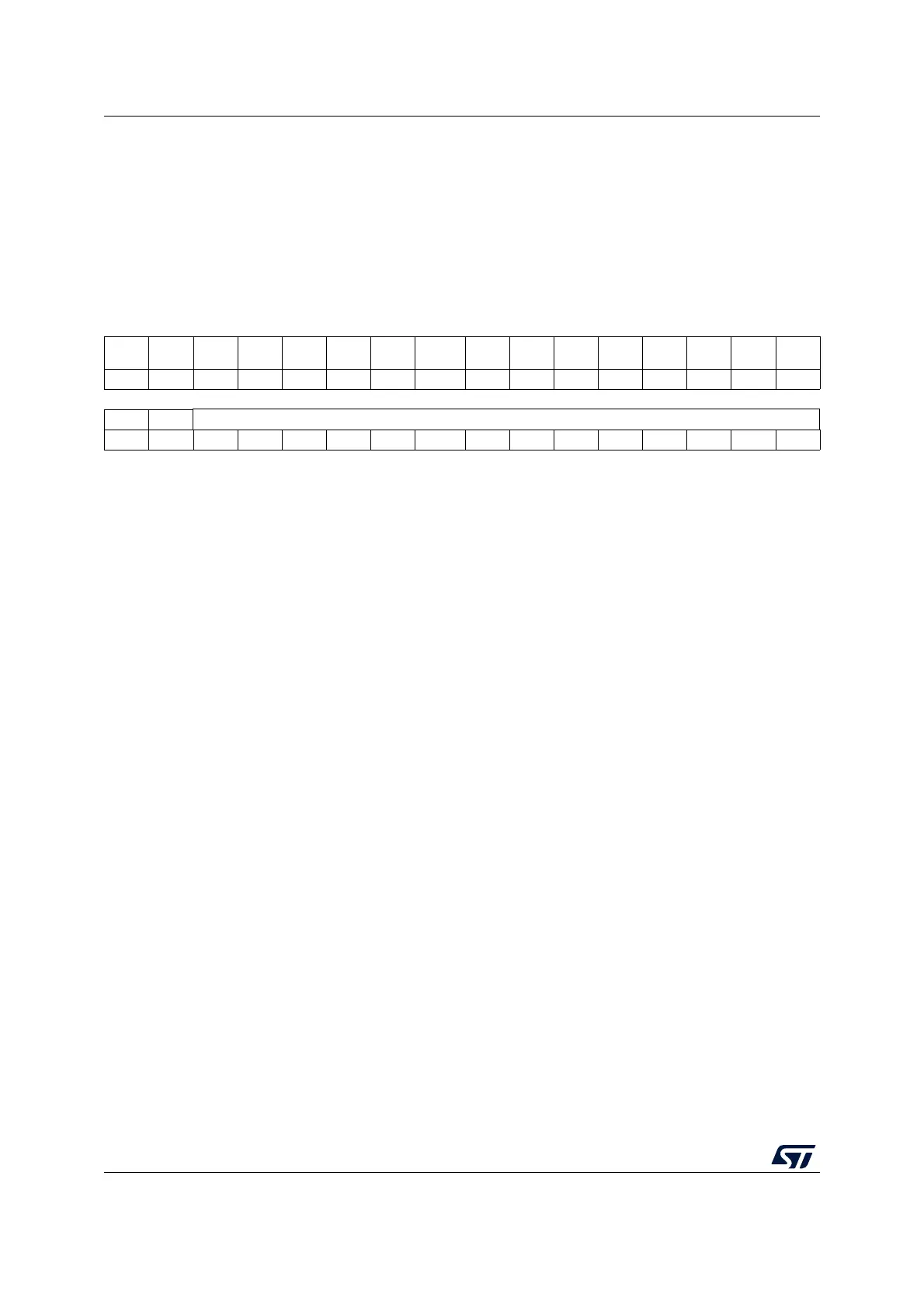
3.7.6 FLASH ECC register (FLASH_ECCR)
Address offset: 0x018
Reset value: 0x0000 0000
Access: no wait state when no Flash memory operation is on going, word, half-word and
byte access
This register applies to single-bank products and to Bank 1 of dual-bank products.
31 30 29 28 27 26 25 24 23 22 21 20 19 18 17 16
ECCD ECCC Res. Res. Res. Res. Res. ECCCIE Res. Res. Res.
SYSF_
ECC
Res. Res. Res. Res.
rc_w1 rc_w1 rw r
1514131211109 8 76543210
Res. Res. ADDR_ECC[13:0]
rrrrr r rrrrrrrr
Bit 31 ECCD: ECC detection
Set by hardware when two ECC errors have been detected. When this bit is set, a NMI is
generated.
Cleared by writing 1.
Bit 30 ECCC: ECC correction
Set by hardware when one ECC error has been detected and corrected. An interrupt is
generated if ECCIE is set.
Cleared by writing 1.
Bits 29:25 Reserved, must be kept at reset value.
Bit 24 ECCCIE: ECC correction interrupt enable
0: ECCC interrupt disabled
1: ECCC interrupt enabled
Bits 23:21 Reserved, must be kept at reset value.
Bit 20 SYSF_ECC: System Flash memory ECC fail
This bit indicates that the ECC error correction or double ECC error detection is located in
the system Flash memory.
Bits 19:14 Reserved, must be kept at reset value.
Bits 13:0 ADDR_ECC[13:0]: ECC fail double-word address offset
In case of ECC error or ECC correction detected, this bitfield contains double-word offset
(multiple of 64 bits) to Main Flash memory.

 Loading...


