RM0444 Rev 5 175/1390
RM0444 Reset and clock control (RCC)
220
TIM16
By setting the TI1SEL[3:0] field of the TIM16_TISEL register, the clock selected for the input
capture channel1 of TIM16 can be one of:
• GPIO (refer to the alternate function mapping in the device datasheets).
• LSI clock
• LSE clock
• RTC wakeup interrupt signal
The last option requires to enable the RTC interrupt.
Figure 13. Frequency measurement with TIM16 in capture mode
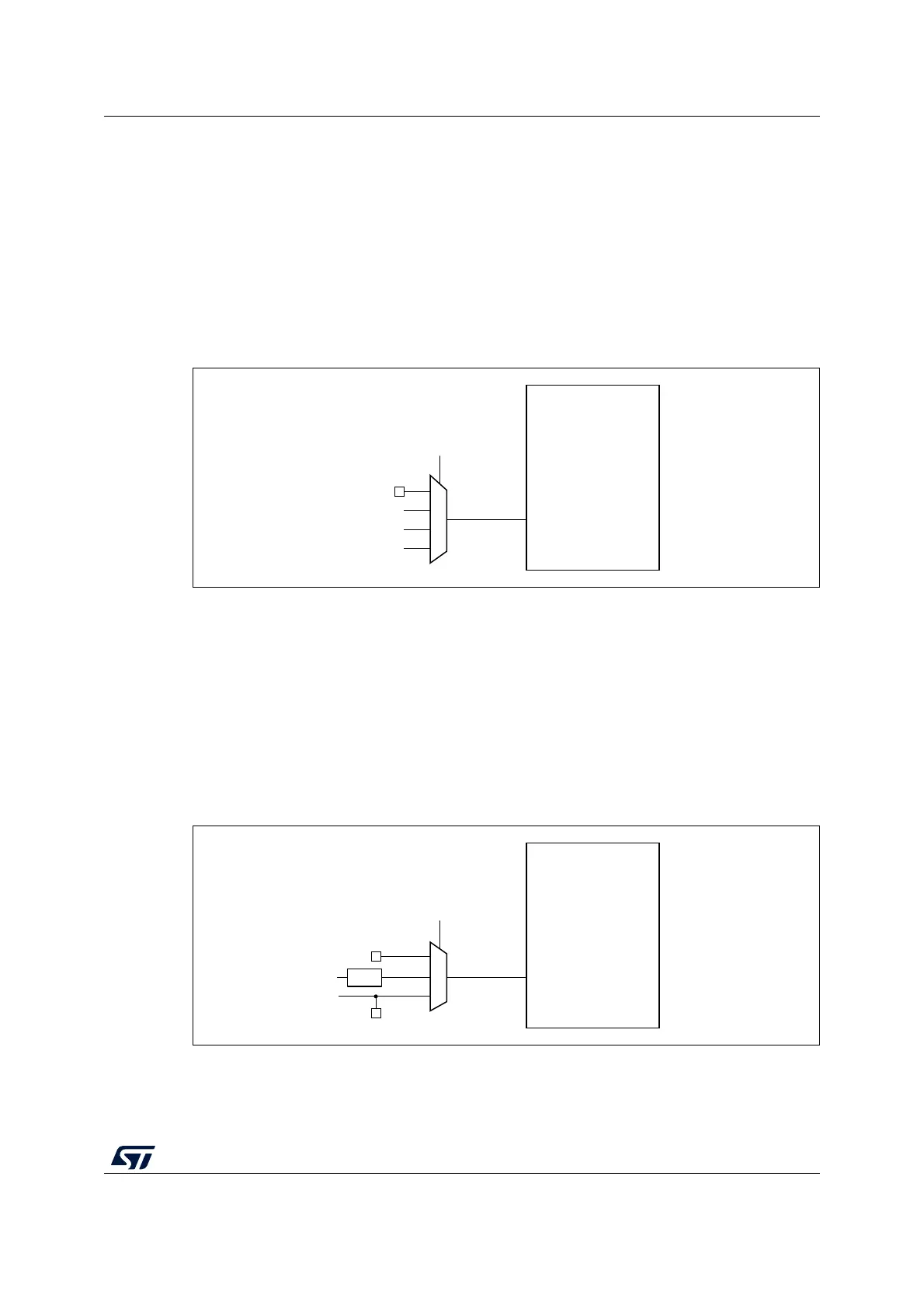
TIM17
By setting the TI1SEL[3:0] field of the TIM17_TISEL register, the clock selected for the input
capture channel1 of TIM17 can be one of:
• GPIO Refer to the alternate function mapping in the device datasheets.
• HSE divided by 32
• MCO (MCU clock output)
The last option is controlled by the MCOSEL[3:0] field of the clock configuration register
(RCC_CFGR). All clock sources can be selected for the MCO pin.
Figure 14. Frequency measurement with TIM17 in capture mode
MSv42175V1
TIM 16
TI1
TI1SEL[3:0]
GPIO
LSE
RTC wakeup interrupt
LSI
MSv42176V1
TIM 17
TI1
TI1SEL[3:0]
GPIO
HSE
MCO
/ 32

 Loading...


