Clock recovery system (CRS) RM0444
222/1390 RM0444 Rev 5
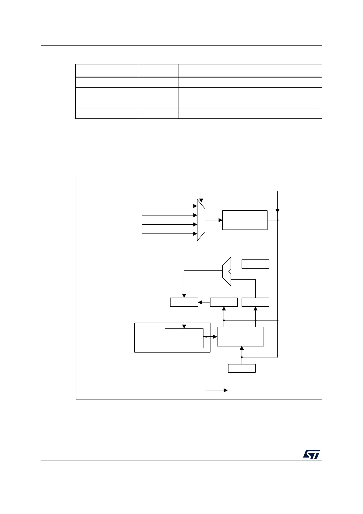
6.4 CRS functional description
6.4.1 CRS block diagram
Figure 15. CRS block diagram
6.4.2 Synchronization input
For more information on the CRS synchronization source configuration, refer to
Section 6.7.2: CRS configuration register (CRS_CFGR).
Table 38. CRS internal input/output signals
Internal signal name Signal type Description
crs_sync_in_1 Input 00: GPIO AF selected as SYNC signal source
crs_sync_in_2 Input 01: LSE selected as SYNC signal source
crs_sync_in_3 Input 10: USB SOF selected as SYNC signal source (default)
crs_sync_in_4 Input 11: Reserved
MS53564V1
SYNCSRC
SYNC divider
(/1, /2, /4,…, /128)
SWSYNC
RELOAD
SYNC
16-bit counter
FECAP
RC 48 MHz
HSI48
RCC
crs_sync_in_1
FELIM
TRIM FEDIR
To peripherals
crs_sync_in_2
crs_sync_in_3
crs_sync_in_4

 Loading...


