Embedded Flash memory (FLASH) RM0444
110/1390 RM0444 Rev 5
3.7.9 FLASH PCROP area A start address register
(FLASH_PCROP1ASR)
Address offset: 0x024
Reset value: 0b0000 0000 0000 0000 0000 000X XXXX XXXX (The option bits are loaded
with values from Flash memory at power-on reset release.)
Access: no wait state when no Flash memory operation is on going, word, half-word access
This register applies to single-bank devices and to Bank 1 of dual-bank devices.
3.7.10 FLASH PCROP area A end address register
(FLASH_PCROP1AER)
Address offset: 0x028
Reset value: 0bX000 0000 0000 0000 0000 000X XXXX XXXX (The option bits are loaded
with values from Flash memory at power-on reset release.)
Access: no wait state when no Flash memory operation is on going, word, half-word access.
PCROP_RDP bit can be accessed with byte access
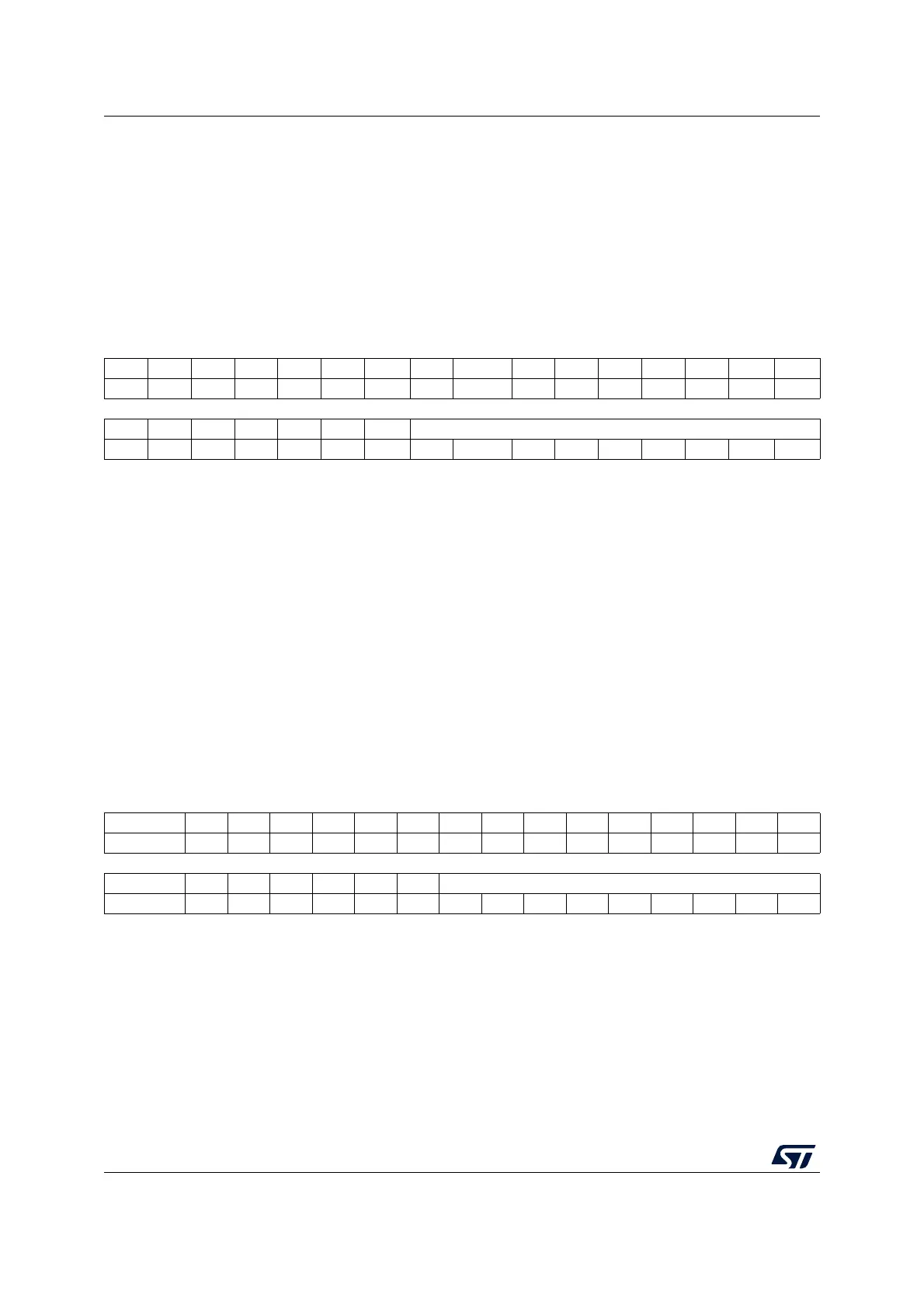
31 30 29 28 27 26 25 24 23 22 21 20 19 18 17 16
Res. Res. Res. Res. Res. Res. Res. Res. Res. Res. Res. Res. Res. Res. Res. Res.
15 14 13 12 11 10 9 8 7 6 5 4 3 2 1 0
Res. Res. Res. Res. Res. Res. Res. PCROP1A_STRT[8:0]
rw rw rw rw rw rw rw rw rw
Bits 31:9 Reserved, must be kept cleared
Bits 8:0 PCROP1A_STRT[8:0]: PCROP1A area start offset (Bank 1)
Contains the offset of the first subpage of the PCROP1A area (in Bank 1 for dual-bank
devices).
(1)
1. The number of effective bits depends on the size of Flash memory in the device.
31 30 29 28 27 26 25 24 23 22 21 20 19 18 17 16
PCROP_RDP Res. Res. Res. Res. Res. Res. Res. Res. Res. Res. Res. Res. Res. Res. Res.
rs
15 14131211109876543210
Res. Res. Res. Res. Res. Res. Res. PCROP1A_END[8:0]
rw rw rw rw rw rw rw rw rw

 Loading...


