Advanced-control timer (TIM1) RM0444
620/1390 RM0444 Rev 5
Note: Refer to Figure 144: Break and Break2 circuitry overview.
21.4.29 TIM1 timer input selection register (TIM1_TISEL)
Address offset: 0x68
Reset value: 0x0000 0000
Bit 3 BK2CMP3E: BRK2 COMP3 enable
This bit enables the COMP3 for the timer’s BRK2 input. COMP3 output is ‘ORed’ with the
other BRK2 sources.
0: COMP3 input disabled
1: COMP3 input enabled
Note: This bit can not be modified as long as LOCK level 1 has been programmed (LOCK bits
in TIMx_BDTR register).
Note: This bit is available on STM32G0B1xx and STM32G0C1xx salestypes only), reserved
otherwise.
Bit 2 BK2CMP2E: BRK2 COMP2 enable
This bit enables the COMP2 for the timer’s BRK2 input. COMP2 output is ‘ORed’ with the
other BRK2 sources.
0: COMP2 input disabled
1: COMP2 input enabled
Note: This bit can not be modified as long as LOCK level 1 has been programmed (LOCK bits
in TIMx_BDTR register).
Bit 1 BK2CMP1E: BRK2 COMP1 enable
This bit enables the COMP1 for the timer’s BRK2 input. COMP1 output is ‘ORed’ with the
other BRK2 sources.
0: COMP1 input disabled
1: COMP1 input enabled
Note: This bit can not be modified as long as LOCK level 1 has been programmed (LOCK bits
in TIMx_BDTR register).
Bit 0 BK2INE: BRK2 BKIN input enable
This bit enables the BKIN2 alternate function input for the timer’s BRK2 input. BKIN2 input is
‘ORed’ with the other BRK2 sources.
0: BKIN2 input disabled
1: BKIN2 input enabled
Note: This bit can not be modified as long as LOCK level 1 has been programmed (LOCK bits
in TIMx_BDTR register).
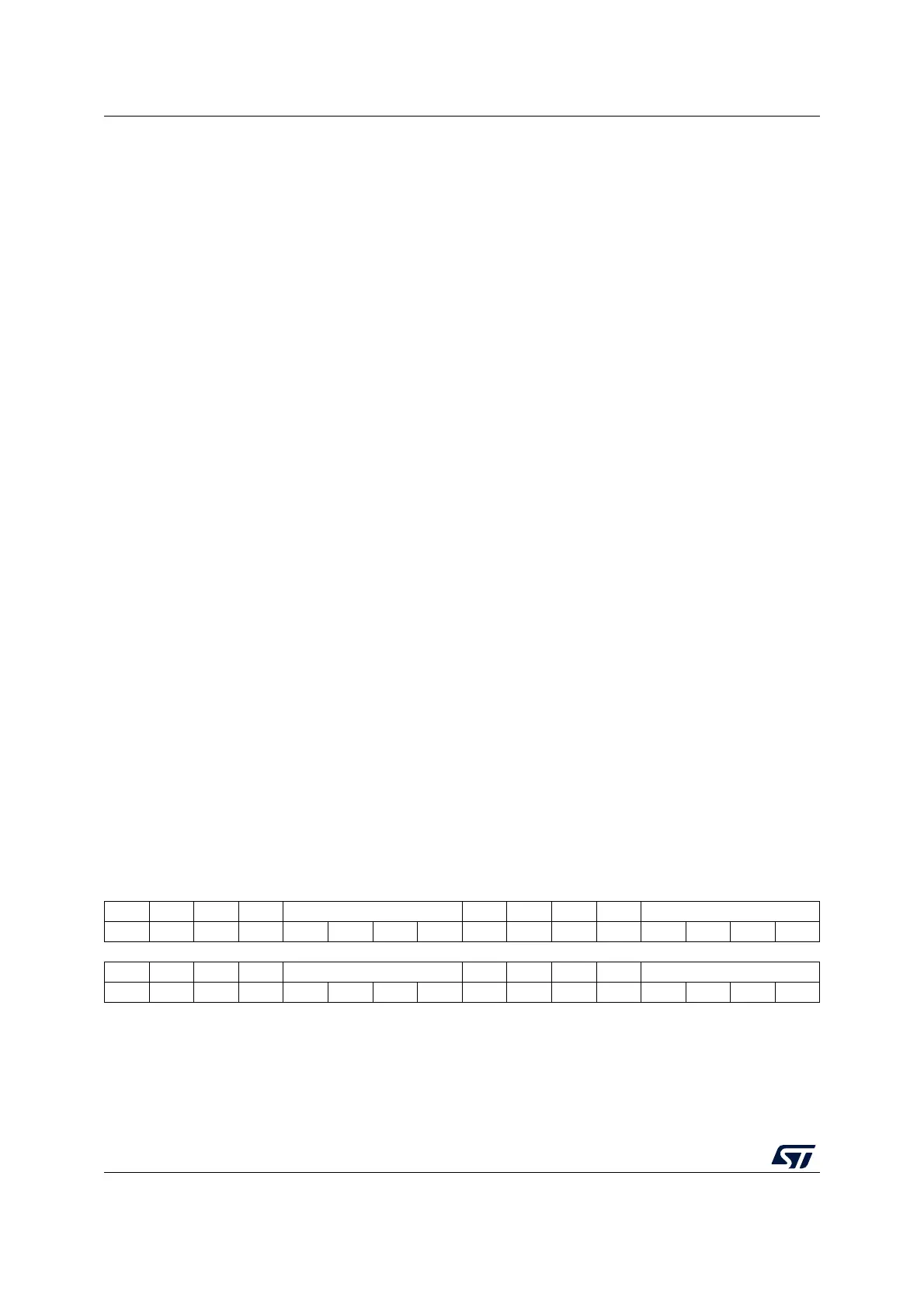
31 30 29 28 27 26 25 24 23 22 21 20 19 18 17 16
Res. Res. Res. Res. TI4SEL[3:0] Res. Res. Res. Res. TI3SEL[3:0]
rw rw rw rw rw rw rw rw
1514131211109876543210
Res. Res. Res. Res. TI2SEL[3:0] Res. Res. Res. Res. TI1SEL[3:0]
rw rw rw rw rw rw rw rw
Bits 31:28 Reserved, must be kept at reset value.
Bits 27:24 TI4SEL[3:0]: selects TI4[0] to TI4[15] input
0000: TIM1_CH4 input
Others: Reserved

 Loading...


