Power control (PWR) RM0444
144/1390 RM0444 Rev 5
4.4.2 Power control register 2 (PWR_CR2)
Address offset: 0x04
Reset value: 0x0000 0000. This register is reset when exiting Standby mode.
Bit 4 FPD_LPRUN: Flash memory powered down during Low-power run mode
This bit determines whether the Flash memory is put in power-down mode or remains in idle
mode when the device enters Low-power run mode. The Flash memory can be put in power-
down mode only when the user code is executed from SRAM.
0: Flash memory idle
1: Flash memory powered down
Bit 3 FPD_STOP: Flash memory powered down during Stop mode
This bit determines whether the Flash memory is put in power-down mode or remains in idle
mode when the device enters Stop mode.
0: Flash memory idle
1: Flash memory powered down
Bits 2:0 LPMS[2:0]: Low-power mode selection
These bits select the low-power mode entered when CPU enters deepsleep mode.
000: Stop 0 mode
001: Stop 1 mode
010: Reserved
011: Standby mode
1xx: Shutdown mode
Note: In Standby mode, SRAM contents are retained or not, depending on
RRS bit setting in PWR_CR3.
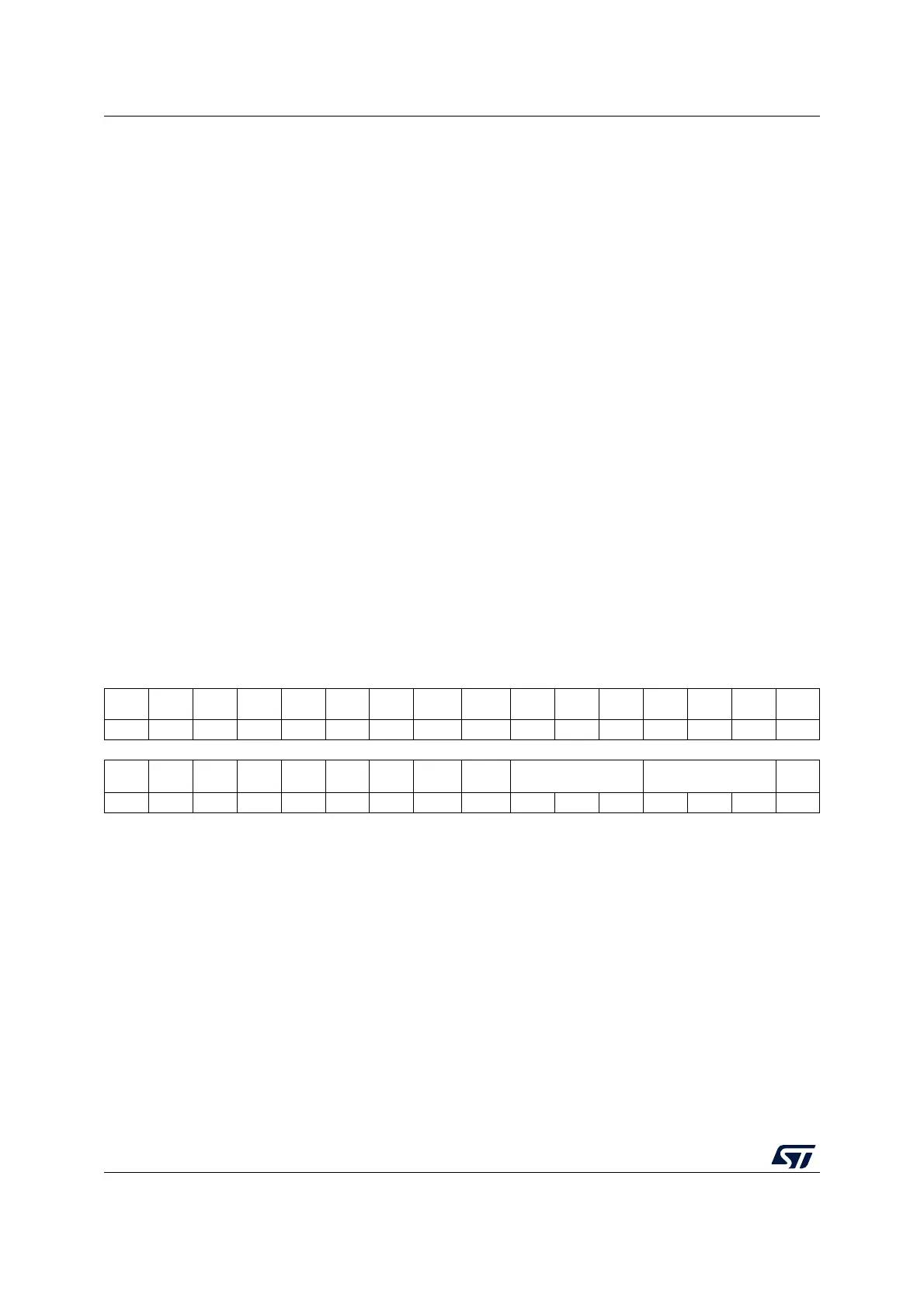
31 30 29 28 27 26 25 24 23 22 21 20 19 18 17 16
Res. Res. Res. Res. Res. Res. Res. Res. Res. Res. Res. Res. Res. Res. Res. Res.
1514131211109 8 7 6543210
Res. Res. Res. Res. Res. USV IOSV
PVMEN
USB
PVMEN
DAC
PVDRT[2:0] PVDFT[2:0] PVDE
rw rw rw rw rw rw rw rw rw rw rw
Bits 31:11 Reserved, must be kept at reset value.
Bit 10 USV: USB supply enable
0: Disable
1: Enable
The bit must be set for the USB peripheral to operate.
Bit 9 IOSV: V
DDIO2
monitoring enable
0: Disable
1: Enable
Setting the bit allows monitoring the V
DDIO2
supply voltage through the PVMOUT flag in the
PWR_SR2 register.

 Loading...


