Comparator (COMP) RM0444
446/1390 RM0444 Rev 5
18.3 COMP functional description
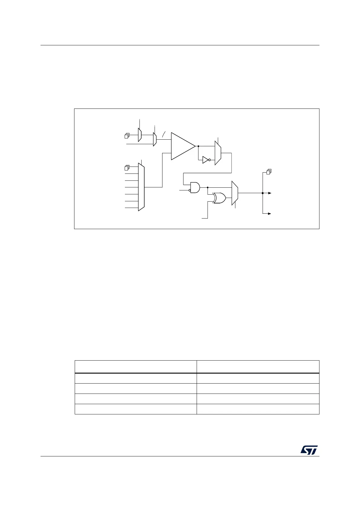
18.3.1 COMP block diagram
The block diagram of the comparators is shown in Figure 68.
Figure 68. Comparator block diagram
18.3.2 COMP pins and internal signals
The I/Os used as comparators inputs must be configured in analog mode in the GPIOs
registers.
The comparator output can be connected to the I/Os using the alternate function channel
given in “Alternate function mapping” table in the datasheet.
The output can also be internally redirected to a variety of timer input for the following
purposes:
• Emergency shut-down of PWM signals, using BKIN and BKIN2 inputs
• Cycle-by-cycle current control, using OCREF_CLR inputs
• Input capture for timing measures
It is possible to have the comparator output simultaneously redirected internally and
externally.
MSv42190V1
COMPx_INM I/Os
COMPx_INP I/Os
1/4 V
REFINT
3/4 V
REFINT
1/2 V
REFINT
V
REFINT
DAC_CH1
DAC_CH2
COMPx_INP
COMPx_INM
Wakeup
EXTI line
interrupt
COMPx
POLARITY
COMPx OUT
COMPx_OUT
COMPx INMSEL
TIMERS
GPIO alternate
function
+
-
COMPx
COMPx INPSEL
COMPy_INP
COMPx WINMODE
Blank source
COMPx WINOUT
COMPx_VALUE
COMPy_VALUE
Table 90. COMP1 non-inverting input assignment
COMP1_INP COMP1_INPSEL[1:0]
PC5 00
PB2 01
PA1 10
Open 11

 Loading...


