Embedded Flash memory (FLASH) RM0444
88/1390 RM0444 Rev 5
PCROP2B start address option bytes
Flash memory address: 0x1FFF 7858
Reset value: 0xFFFF FFFF (ST production value)
The register pertains to dual-bank devices only. In single-bank devices, it is reserved.
PCROP2B end address option bytes
Flash memory address: 0x1FFF 7860
Reset value: 0x0000 0000 (ST production value)
The register pertains to dual-bank devices only. In single-bank devices, it is reserved.
Bits 31:23 Reserved, must be kept at reset value.
Bits 22:16 WRP2B_END[6:0]: WRP area B end offset, Bank 2
WRP2B_END contains the offset of the last page of the WRP area B in Bank 2 of dual-bank
devices.
Note: Values corresponding to addresses outside the Main memory are not allowed.
Bits 15:7 Reserved, must be kept at reset value.
Bits 6:0 WRP2B_STRT[6:0]: WRP area B start offset
WRP2B_STRT contains the offset of the first page of the WRP area B in Bank 2 of dual-
bank devices.
Note: Values corresponding to addresses outside the Main memory are not allowed.
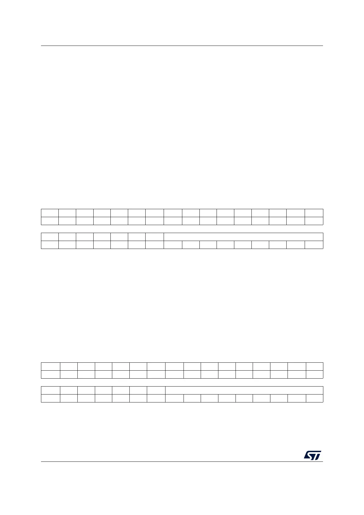
31 30 29 28 27 26 25 24 23 22 21 20 19 18 17 16
Res. Res. Res. Res. Res. Res. Res. Res. Res. Res. Res. Res. Res. Res. Res. Res.
1514131211109 8 765432 1 0
Res. Res. Res. Res. Res. Res. Res. PCROP2B_STRT[8:0]
rrrrrr r r
Bits 31:9 Reserved, must be kept at reset value.
Bits 8:0 PCROP2B_STRT[8:0]: PCROP2B area start offset, Bank 2
PCROP2B_STRT contains the offset of the first PCROP subpage of the PCROP2B area in
Bank 2 of dual-bank devices.
Note: Values corresponding to addresses outside the Main memory are not allowed.
31 30 29 28 27 26 25 24 23 22 21 20 19 18 17 16
Res. Res. Res. Res. Res. Res. Res. Res. Res. Res. Res. Res. Res. Res. Res. Res.
15 14 13 12 11 10 9 8 7 6 5 4 3 2 1 0
Res. Res. Res. Res. Res. Res. Res. PCROP2B_END[8:0]
r rrrrrr rr

 Loading...


