phase A input
system clock
phase B input
synchronizer
CH0FVAL[3:0]
PHAFLTREN
filtered phase A signal
PHAPOL PHBPOL
filtered phase B signal
PHBFLTREN
CH1FVAL[3:0]
synchronizer
Filter
CLK
D
Q
CLK
D
Q
CLK
D
Q
CLK
D
Q
Filter
Filter
FTM counter
direction
FTM counter
enable
up/down
CNTIN
MOD
TOFDIR
QUADIR
0
1
0
1
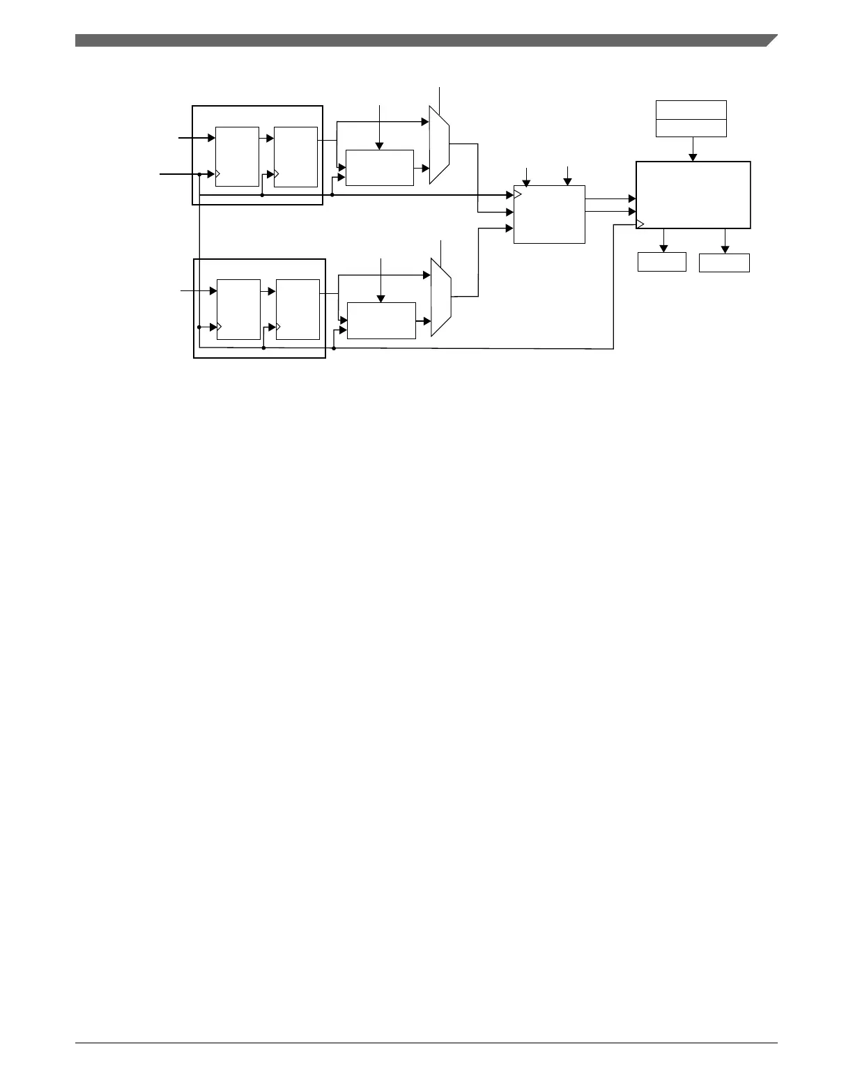
Figure 39-89. Quadrature Decoder block diagram
Each one of input signals phase A and B has a filter that is equivalent to the filter used in
the channels input; Filter for Input Capture mode. The phase A input filter is enabled by
PHAFLTREN bit and this filter’s value is defined by CH0FVAL[3:0] bits
(CH(n)FVAL[3:0] bits in FILTER0 register). The phase B input filter is enabled by
PHBFLTREN bit and this filter’s value is defined by CH1FVAL[3:0] bits (CH(n
+1)FVAL[3:0] bits in FILTER0 register).
Except for CH0FVAL[3:0] and CH1FVAL[3:0] bits, no channel logic is used in
Quadrature Decoder mode.
Note
Notice that the FTM counter is clocked by the phase A and B
input signals when quadrature decoder mode is selected.
Therefore it is expected that the Quadrature Decoder be used
only with the FTM channels in input capture or output compare
modes.
Note
An edge at phase A must not occur together an edge at phase B
and vice-versa.
The PHAPOL bit selects the polarity of the phase A input, and the PHBPOL bit selects
the polarity of the phase B input.
Chapter 39 FlexTimer Module (FTM)
K22F Sub-Family Reference Manual, Rev. 4, 08/2016
NXP Semiconductors 1015

 Loading...