PORT memory map (continued)
Absolute
address
(hex)
Register name
Width
(in bits)
Access Reset value
Section/
page
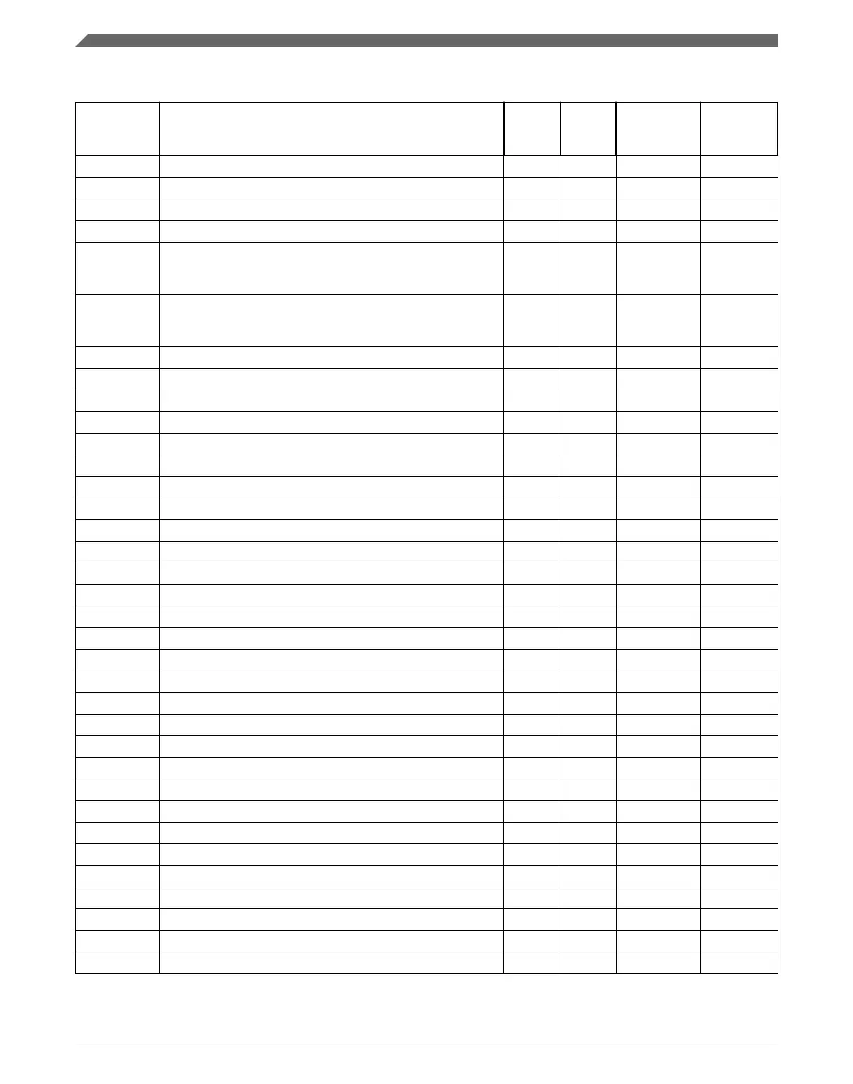
4004_C070 Pin Control Register n (PORTD_PCR28) 32 R/W See section 11.5.1/248
4004_C074 Pin Control Register n (PORTD_PCR29) 32 R/W See section 11.5.1/248
4004_C078 Pin Control Register n (PORTD_PCR30) 32 R/W See section 11.5.1/248
4004_C07C Pin Control Register n (PORTD_PCR31) 32 R/W See section 11.5.1/248
4004_C080 Global Pin Control Low Register (PORTD_GPCLR) 32
W
(always
reads 0)
0000_0000h 11.5.2/251
4004_C084 Global Pin Control High Register (PORTD_GPCHR) 32
W
(always
reads 0)
0000_0000h 11.5.3/251
4004_C0A0 Interrupt Status Flag Register (PORTD_ISFR) 32 w1c 0000_0000h 11.5.4/252
4004_C0C0 Digital Filter Enable Register (PORTD_DFER) 32 R/W 0000_0000h 11.5.5/252
4004_C0C4 Digital Filter Clock Register (PORTD_DFCR) 32 R/W 0000_0000h 11.5.6/253
4004_C0C8 Digital Filter Width Register (PORTD_DFWR) 32 R/W 0000_0000h 11.5.7/253
4004_D000 Pin Control Register n (PORTE_PCR0) 32 R/W See section 11.5.1/248
4004_D004 Pin Control Register n (PORTE_PCR1) 32 R/W See section 11.5.1/248
4004_D008 Pin Control Register n (PORTE_PCR2) 32 R/W See section 11.5.1/248
4004_D00C Pin Control Register n (PORTE_PCR3) 32 R/W See section 11.5.1/248
4004_D010 Pin Control Register n (PORTE_PCR4) 32 R/W See section 11.5.1/248
4004_D014 Pin Control Register n (PORTE_PCR5) 32 R/W See section 11.5.1/248
4004_D018 Pin Control Register n (PORTE_PCR6) 32 R/W See section 11.5.1/248
4004_D01C Pin Control Register n (PORTE_PCR7) 32 R/W See section 11.5.1/248
4004_D020 Pin Control Register n (PORTE_PCR8) 32 R/W See section 11.5.1/248
4004_D024 Pin Control Register n (PORTE_PCR9) 32 R/W See section 11.5.1/248
4004_D028 Pin Control Register n (PORTE_PCR10) 32 R/W See section 11.5.1/248
4004_D02C Pin Control Register n (PORTE_PCR11) 32 R/W See section 11.5.1/248
4004_D030 Pin Control Register n (PORTE_PCR12) 32 R/W See section 11.5.1/248
4004_D034 Pin Control Register n (PORTE_PCR13) 32 R/W See section 11.5.1/248
4004_D038 Pin Control Register n (PORTE_PCR14) 32 R/W See section 11.5.1/248
4004_D03C Pin Control Register n (PORTE_PCR15) 32 R/W See section 11.5.1/248
4004_D040 Pin Control Register n (PORTE_PCR16) 32 R/W See section 11.5.1/248
4004_D044 Pin Control Register n (PORTE_PCR17) 32 R/W See section 11.5.1/248
4004_D048 Pin Control Register n (PORTE_PCR18) 32 R/W See section 11.5.1/248
4004_D04C Pin Control Register n (PORTE_PCR19) 32 R/W See section 11.5.1/248
4004_D050 Pin Control Register n (PORTE_PCR20) 32 R/W See section 11.5.1/248
4004_D054 Pin Control Register n (PORTE_PCR21) 32 R/W See section 11.5.1/248
4004_D058 Pin Control Register n (PORTE_PCR22) 32 R/W See section 11.5.1/248
4004_D05C Pin Control Register n (PORTE_PCR23) 32 R/W See section 11.5.1/248
4004_D060 Pin Control Register n (PORTE_PCR24) 32 R/W See section 11.5.1/248
Table continues on the next page...
Memory map and register definition
K22F Sub-Family Reference Manual, Rev. 4, 08/2016
246 NXP Semiconductors

 Loading...