UM10360 All information provided in this document is subject to legal disclaimers. © NXP B.V. 2013. All rights reserved.
User manual Rev. 3 — 19 December 2013 94 of 841
NXP Semiconductors
UM10360
Chapter 7: LPC176x/5x Pin configuration
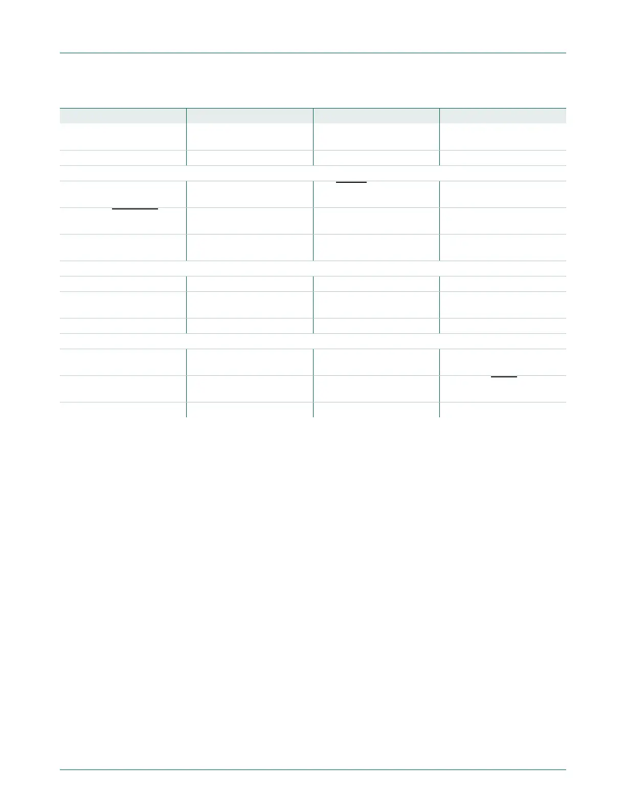
5 P0[23]/AD0[0]/
I2SRX_CLK/CAP3[0]
6 P4[29]/TX_MCLK/
MAT2[1]/RXD3
7 P2[3]/PWM1[4]/
DCD1/TRACEDATA[2]
8 P2[6]/PCAP1[0]/
RI1/TRACECLK
9 P2[7]/RD2/RTS1 10 P2[8]/TD2/TXD2 11 - 12 -
Row F
1 VREFN 2 RTCX1 3 RESET 4 P1[31]/SCK1/
AD0[5]
5 P1[21]/MCABORT
/
PWM1[3]/SSEL0
6 P0[18]/DCD1/
MOSI0/MOSI
7 P2[9]/USB_CONNECT/
RXD2
8 P0[16]/RXD1/
SSEL0/SSEL
9 P0[17]/CTS1/
MISO0/MISO
10 P0[15]/TXD1/
SCK0/SCK
11 - 12 -
Row G
1 RTCX2 2 VBAT 3 XTAL2 4 P0[30]/USB_D
5 P1[25]/MCOA1/
MAT1[1]
6P1[29]/MCOB2/
PCAP1[1]/MAT0[1]
7V
SS
8 P0[21]/RI1/RD1
9 P0[20]/DTR1/SCL1 10 P0[19]/DSR1/SDA1 11 - 12 -
Row H
1 P1[30]/V
BUS
/
AD0[4]
2 XTAL1 3 P3[25]/MAT0[0]/
PWM1[2]
4 P1[18]/USB_UP_LED/
PWM1[1]/CAP1[0]
5 P1[24]/MCI2/
PWM1[5]/MOSI0
6V
DD(REG)(3V3)
7 P0[10]/TXD2/
SDA2/MAT3[0]
8P2[11]/EINT1/
I2STX_CLK
9V
DD(3V3)
10 P0[22]/RTS1/TD1 11 - 12 -
Table 72. Pin allocation table TFBGA100 package …continued
Pin Symbol Pin Symbol Pin Symbol Pin Symbol

 Loading...


