• Flash address space divided into (32 or 64) equal-sized segments (segment size is
defined as flash_size [bytes]/(32 or 64))
• Separate control bits for supervisor-only access and execute-only access per segment
• Access control evaluated on each bus cycle routed to the flash
• Access violation errors terminate the bus cycle and return zeroes for read data
• Programming model allows 2 levels of protected segments
28.5.4.1 Memory map and register definitions
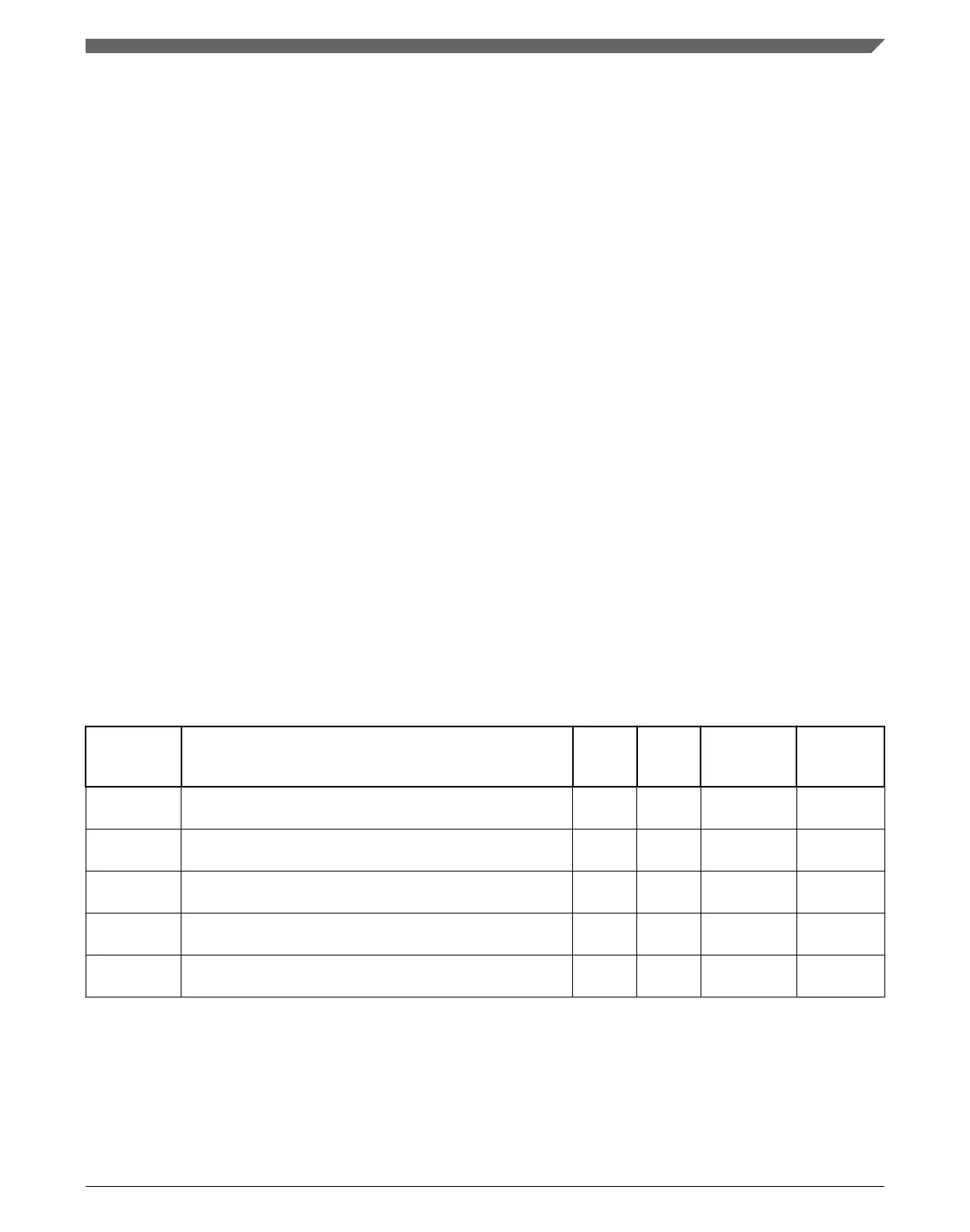
The following table shows the mapping of FAC registers. Descriptions of each register
and its bit assignments follow.
• The Flash Management Unit (FMU) supports access to its FAC programming model
via a 32-bit slave peripheral bus connection.
• Unimplemented register bits read as zero.
• For implementations supporting only 32 segments, only the 32-bit "low" register is
implemented.
• Writes to any read-only or reserved registers are ignored; attempts to access flash
register space above offset '2B' will generate a transfer error.
•
The terms supervisor and user modes are equivalent to privileged and unprivileged
modes.
•
In this FAC section, n refers to the segment number, and x is the acronym of the
module that the registers are in (which sometimes varies from one device to another).
x memory map
Absolute
address
(hex)
Register name
Width
(in bits)
Access Reset value
Section/
page
18 Execute-only Access Register High (x_XACCH) 32 R See section
28.5.4.1.1/
618
1C Execute-only Access Register Low (x_XACCL) 32 R See section
28.5.4.1.2/
618
20 Supervisor-only Access Register High (x_SACCH) 32 R See section
28.5.4.1.3/
619
24 Supervisor-only Access Register Low (x_SACCL) 32 R See section
28.5.4.1.4/
620
28 Configuration Register (x_CR) 32 R See section
28.5.4.1.5/
620
Chapter 28 Flash Memory Controller (FMC)
K22F Sub-Family Reference Manual, Rev. 4, 08/2016
NXP Semiconductors 617

 Loading...