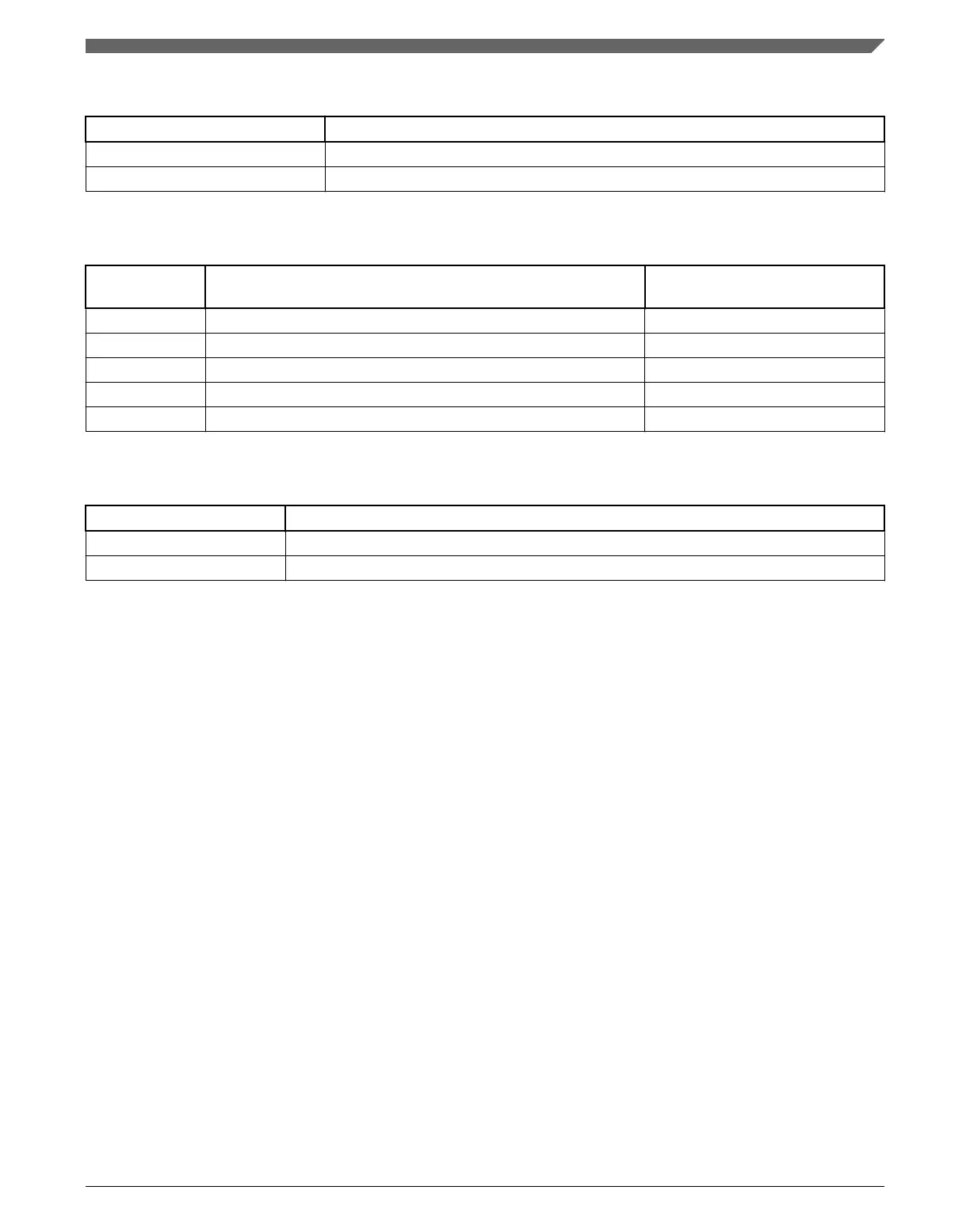
Table 34-5. Base conversion time (BCT) (continued)
Mode Base conversion time (BCT)
16b single-ended 25 ADCK cycles
16b differential 34 ADCK cycles
Table 34-6. Long sample time adder (LSTAdder)
CFG1[ADLSMP] CFG2[ADLSTS]
Long sample time adder
(LSTAdder)
0 xx 0 ADCK cycles
1 00 20 ADCK cycles
1 01 12 ADCK cycles
1 10 6 ADCK cycles
1 11 2 ADCK cycles
Table 34-7. High-speed conversion time adder (HSCAdder)
CFG2[ADHSC] High-speed conversion time adder (HSCAdder)
0 0 ADCK cycles
1 2 ADCK cycles
Note
The ADCK frequency must be between f
ADCK
minimum and
f
ADCK
maximum to meet ADC specifications.
34.4.4.6
Conversion time examples
The following examples use the Equation 1 on page 796, and the information provided in
Table 34-3 through Table 34-7.
34.4.4.6.1
Typical conversion time configuration
A typical configuration for ADC conversion is:
• 10-bit mode, with the bus clock selected as the input clock source
• The input clock divide-by-1 ratio selected
• Bus frequency of 8 MHz
• Long sample time disabled
• High-speed conversion disabled
Chapter 34 Analog-to-Digital Converter (ADC)
K22F Sub-Family Reference Manual, Rev. 4, 08/2016
NXP Semiconductors 797

 Loading...