UM10360 All information provided in this document is subject to legal disclaimers. © NXP B.V. 2013. All rights reserved.
User manual Rev. 3 — 19 December 2013 487 of 841
NXP Semiconductors
UM10360
Chapter 20: LPC176x/5x I2S
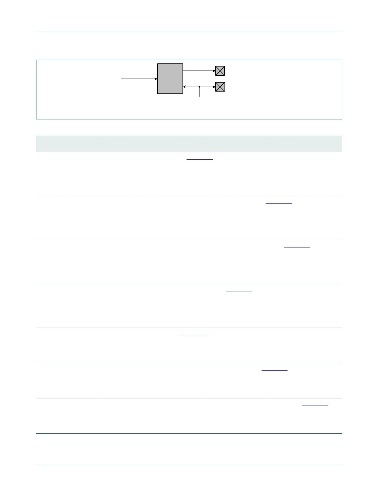
Fig 106. 4-wire transmitter slave mode sharing the receiver bit clock and WS
I2STX_WS
I2STX_SDA
RX bit clock
RX_WS ref
I
2
S
peripheral
block
(transmit)
Table 420: I
2
S receive modes
I2SDAI
[5]
I2SRXMODE
[3:0]
Description
0 0 0 0 0 Typical receiver master mode. See Figure 107.
The
I
2
S receive function operates as a master.
The receive clock source is the fractional rate divider.
The WS used is the internally generated RX_WS.
The RX_MCLK pin is not enabled for output.
0 0 0 1 0 Receiver master mode sharing the transmitter reference clock. See Figure 108
.
The
I
2
S receive function operates as a master.
The receive clock source is TX_REF.
The WS used is the internally generated RX_WS.
The RX_MCLK pin is not enabled for output.
0 0 1 0 0 4-wire receiver master mode sharing the transmitter bit clock and WS. See Figure 109
.
The
I
2
S receive function operates as a master.
The receive clock source is the TX bit clock.
The WS used is the internally generated TX_WS.
The RX_MCLK pin is not enabled for output.
0 1 0 0 0 Receiver master mode with RX_MCLK output. See Figure 107
.
The
I
2
S receive function operates as a master.
The receive clock source is the fractional rate divider.
The WS used is the internally generated RX_WS.
The RX_MCLK pin is enabled for output.
1 0 0 0 0 Typical receiver slave mode. See Figure 110
.
The
I
2
S receive function operates as a slave.
The receive clock source is the RX_CLK pin.
The WS used is the RX_WS pin.
1 0 0 1 0 Receiver slave mode sharing the transmitter reference clock. See Figure 111
.
The
I
2
S receive function operates as a slave.
The receive clock source is TX_REF.
The WS used is the RX_WS pin.
1 0 1 0 0 This is a 4-wire receiver slave mode sharing the transmitter bit clock and WS. See Figure 112
.
The
I
2
S receive function operates as a slave.
The receive clock source is the TX bit clock.
The WS used is TX_WS ref.

 Loading...


