RM0444 Rev 5 83/1390
RM0444 Embedded Flash memory (FLASH)
118
PCROP1A start address option bytes
Flash memory address: 0x1FFF 7808
Reset value: 0xFFFF FFFF (ST production value)
Bit 15 nRSTS_SHDW
0: Reset generated when entering the Shutdown mode
1: No reset generated when entering the Shutdown mode
Bit 14 nRST_STDBY
0: Reset generated when entering the Standby mode
1: No reset generate when entering the Standby mode
Bit 13 nRST_STOP
0: Reset generated when entering the Stop mode
1: No reset generated when entering the Stop mode
Bits12:11 BORF_LEV[1:0]: BOR threshold at falling V
DD
supply
Falling V
DD
crossings this threshold activates the reset signal.
00: BOR falling level 1 with threshold around 2.0 V
01: BOR falling level 2 with threshold around 2.2 V
10: BOR falling level 3 with threshold around 2.5 V
11: BOR falling level 4 with threshold around 2.8 V
Bits10:9 BORR_LEV[1:0]: BOR threshold at rising V
DD
supply
Rising V
DD
crossings this threshold releases the reset signal.
00: BOR rising level 1 with threshold around 2.1 V
01: BOR rising level 2 with threshold around 2.3 V
10: BOR rising level 3 with threshold around 2.6 V
11: BOR rising level 4 with threshold around 2.9 V
Bit 8 BOR_EN: Brown out reset enable
0: Configurable brown out reset disabled, power-on reset defined by POR/PDR levels
1: Configurable brown out reset enabled, values of BORR_LEV and BORF_LEV taken into
account
Bits 7:0 RDP[7:0]: Read protection level
0xAA: Level 0, read protection not active
0xCC: Level 2, chip read protection active
Others: Level 1, memories read protection active
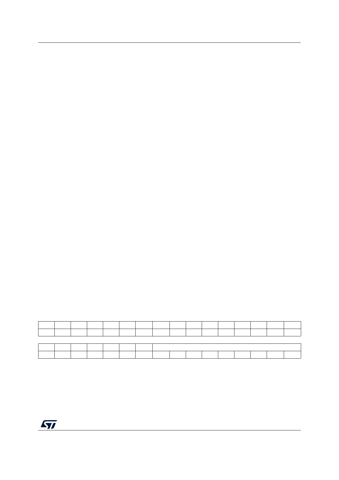
31 30 29 28 27 26 25 24 23 22 21 20 19 18 17 16
Res. Res. Res. Res. Res. Res. Res. Res. Res. Res. Res. Res. Res. Res. Res. Res.
1514131211109 8 765432 1 0
Res. Res. Res. Res. Res. Res. Res. PCROP1A_STRT[8:0]
r rrrrrrr r
Bits 31:9 Reserved, must be kept at reset value.
Bits 8:0 PCROP1A_STRT[8:0]: PCROP1A area start offset (Bank 1)
PCROP1A_STRT contains the offset of the first PCROP subpage of the PCROP1A area (in
Bank 1 for dual-bank devices).
Note: Values corresponding to addresses outside the Main memory are not allowed.

 Loading...


