RM0444 Rev 5 85/1390
RM0444 Embedded Flash memory (FLASH)
118
WRP1B address option bytes
Flash memory address: 0x1FFF 7820
Reset value: 0x0000 00FF (ST production value)
PCROP1B start address option bytes
Flash memory address: 0x1FFF 7828
Reset value: 0xFFFF FFFF (ST production value)
PCROP1B end address option bytes
Flash memory address: 0x1FFF 7830
Reset value: 0x0000 0000 (ST production value)
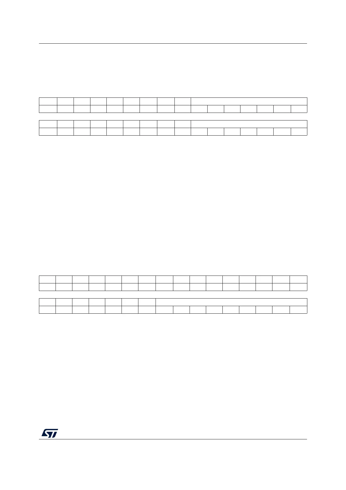
31 30 29 28 27 26 25 24 23 22 21 20 19 18 17 16
Res. Res. Res. Res. Res. Res. Res. Res. Res. WRP1B_END[6:0]
rrrrr rr
15 14 13 12 11 10 9 8 7 6 5 4 3 2 1 0
Res. Res. Res. Res. Res. Res. Res. Res. Res. WRP1B_STRT[6:0]
rrrrr rr
Bits 31:23 Reserved, must be kept at reset value.
Bits 22:16 WRP1B_END[6:0]: WRP area B end offset (Bank 1)
WRP1B_END contains the offset of the last page of the WRP area B (in Bank 1 for dual-
bank devices).
Note: Values corresponding to addresses outside the Main memory are not allowed.
Bits 15:7 Reserved, must be kept at reset value.
Bits 6:0 WRP1B_STRT[6:0]: WRP area B start offset (Bank 1)
WRP1B_STRT contains the offset of the first page of the WRP area B (in Bank 1 for dual-
bank devices).
Note: Values corresponding to addresses outside the Main memory are not allowed.
31 30 29 28 27 26 25 24 23 22 21 20 19 18 17 16
Res. Res. Res. Res. Res. Res. Res. Res. Res. Res. Res. Res. Res. Res. Res. Res.
1514131211109 8 765432 1 0
Res. Res. Res. Res. Res. Res. Res. PCROP1B_STRT[8:0]
r rrrrrrr r
Bits 31:9 Reserved, must be kept at reset value.
Bits 8:0 PCROP1B_STRT[8:0]: PCROP1B area start offset (Bank 1)
PCROP1B_STRT contains the offset of the first PCROP subpage of the PCROP1B area (in
Bank 1 for dual-bank devices).
Note: Values corresponding to addresses outside the Main memory are not allowed.

 Loading...


