Inter-integrated circuit (I2C) interface RM0351
1130/1693 DocID024597 Rev 3
Note: SCLL is also used to generate the t
BUF
and
t
SU:STA
timings.
SCLH is also used to generate the t
HD:STA
and
t
SU:STO
timings.
Refer to Section 35.4.9: I2C_TIMINGR register configuration examples for examples of
I2C_TIMINGR settings vs. I2CCLK frequency.
Master communication initialization (address phase)
In order to initiate the communication, the user must program the following parameters for
the addressed slave in the I2C_CR2 register:
• Addressing mode (7-bit or 10-bit): ADD10
• Slave address to be sent: SADD[9:0]
• Transfer direction: RD_WRN
• In case of 10-bit address read: HEAD10R bit. HEAD10R must be configure to indicate
if the complete address sequence must be sent, or only the header in case of a
direction change.
• The number of bytes to be transferred: NBYTES[7:0]. If the number of bytes is equal to
or greater than 255 bytes, NBYTES[7:0] must initially be filled with 0xFF.
The user must then set the START bit in I2C_CR2 register. Changing all the above bits is
not allowed when START bit is set.
Then the master automatically sends the START condition followed by the slave address as
soon as it detects that the bus is free (BUSY = 0) and after a delay of t
BUF
.
In case of an arbitration loss, the master automatically switches back to slave mode and can
acknowledge its own address if it is addressed as a slave.
Note: The START bit is reset by hardware when the slave address has been sent on the bus,
whatever the received acknowledge value. The START bit is also reset by hardware if an
arbitration loss occurs. If the I2C is addressed as a slave (ADDR=1) while the START bit is
set, the I2C switches to slave mode and the START bit is cleared when the ADDRCF bit is
set.
Note: The same procedure is applied for a Repeated Start condition. In this case BUSY=1.
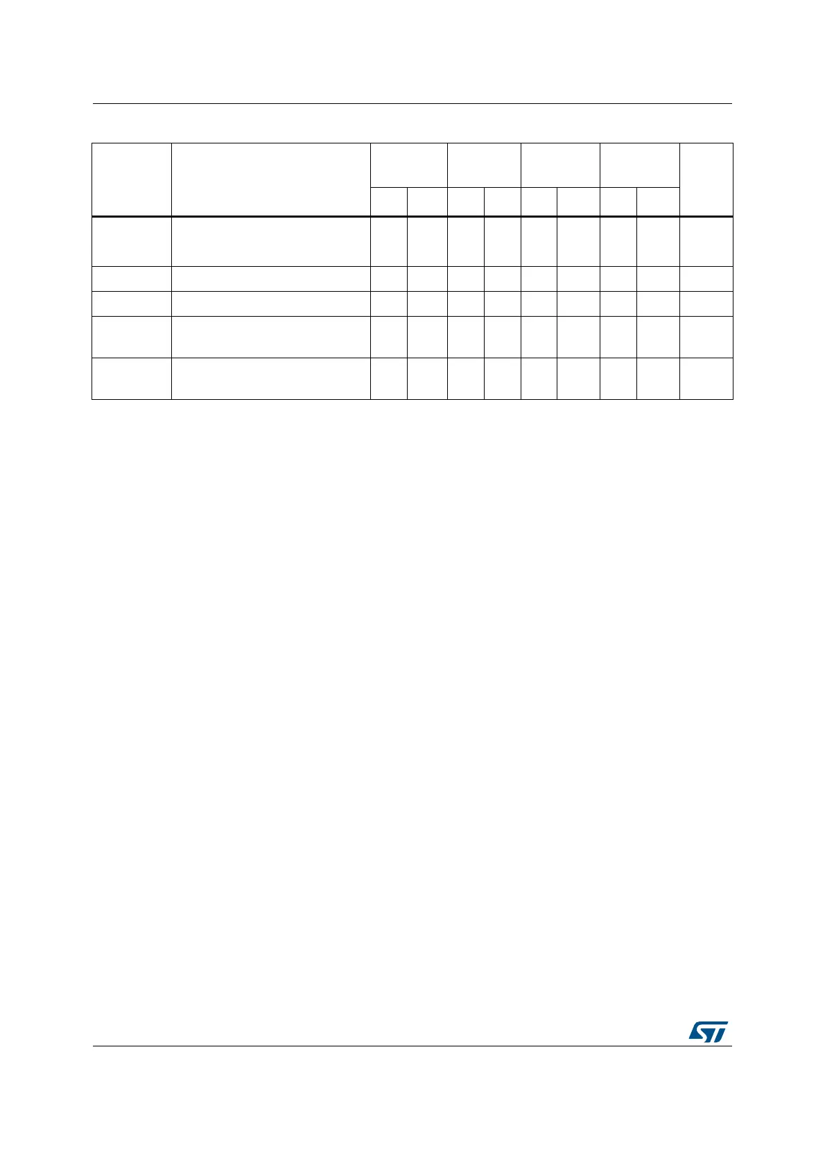
t
BUF
Bus free time between a
STOP and START condition
4.7 - 1.3 0.5 - 4.7 - µs
t
LOW
Low period of the SCL clock
4.7 - 1.3 0.5 - 4.7 - µs
t
HIGH
Period of the SCL clock
4.0 - 0.6 0.26 - 4.0 50 µs
t
r
Rise time of both SDA and
SCL signals
- 1000 - 300 120 - 1000 ns
t
f
Fall time of both SDA and SCL
signals
- 300 - 300 120 - 300 ns
Table 179. I
2
C-SMBUS specification clock timings (continued)
Symbol Parameter
Standard-
mode (Sm)
Fast-mode
(Fm)
Fast-mode
Plus (Fm+)
SMBUS
Unit
Min Max Min Max Min Max Min Max

 Loading...


