DocID024597 Rev 3 631/1693
RM0351 Digital filter for sigma delta modulators (DFSDM)
657
21.6.2 DFSDM channel configuration y register (DFSDM_CHCFGyR2)
(y=0..7)
This register specifies the parameters used by channel y (y = 0..7).
Address offset: 0x04
Reset value: 0x0000 0000
Bit 5 SCDEN: Short-circuit detector enable on channel y
0: Input channel y will not be guarded by the short-circuit detector
1: Input channel y will be continuously guarded by the short-circuit detector
Bit 4 Reserved, must be kept at reset value.
Bits 3:2 SPICKSEL[1:0]: SPI clock select for channel y
0:clock coming from external DFSDM_CKINy input - sampling point according SITP[1:0]
1:clock coming from internal DFSDM_CKOUT output - sampling point according SITP[1:0]
2:clock coming from internal DFSDM_CKOUT - sampling point on each second DFSDM_CKOUT
falling edge.
For connection to external modulator which divides its clock input (from DFSDM_CKOUT) by 2
to generate its output serial communication clock (and this output clock change is active on
each clock input rising edge).
3:clock coming from internal DFSDM_CKOUT output - sampling point on each second
DFSDM_CKOUT rising edge.
For connection to external modulator which divides its clock input (from DFSDM_CKOUT) by 2
to generate its output serial communication clock (and this output clock change is active on each
clock input falling edge).
This value can be modified only when CHEN=0 (in DFSDM_CHCFGyR1 register).
Bits 1:0 SITP[1:0]: Serial interface type for channel y
00: SPI with rising edge to strobe data
01: SPI with falling edge to strobe data
10: Manchester coded input on DFSDM_DATINy pin: rising edge = logic 0, falling edge = logic 1
11: Manchester coded input on DFSDM_DATINy pin: rising edge = logic 1, falling edge = logic 0
This value can only be modified when CHEN=0 (in DFSDM_CHCFGyR1 register).
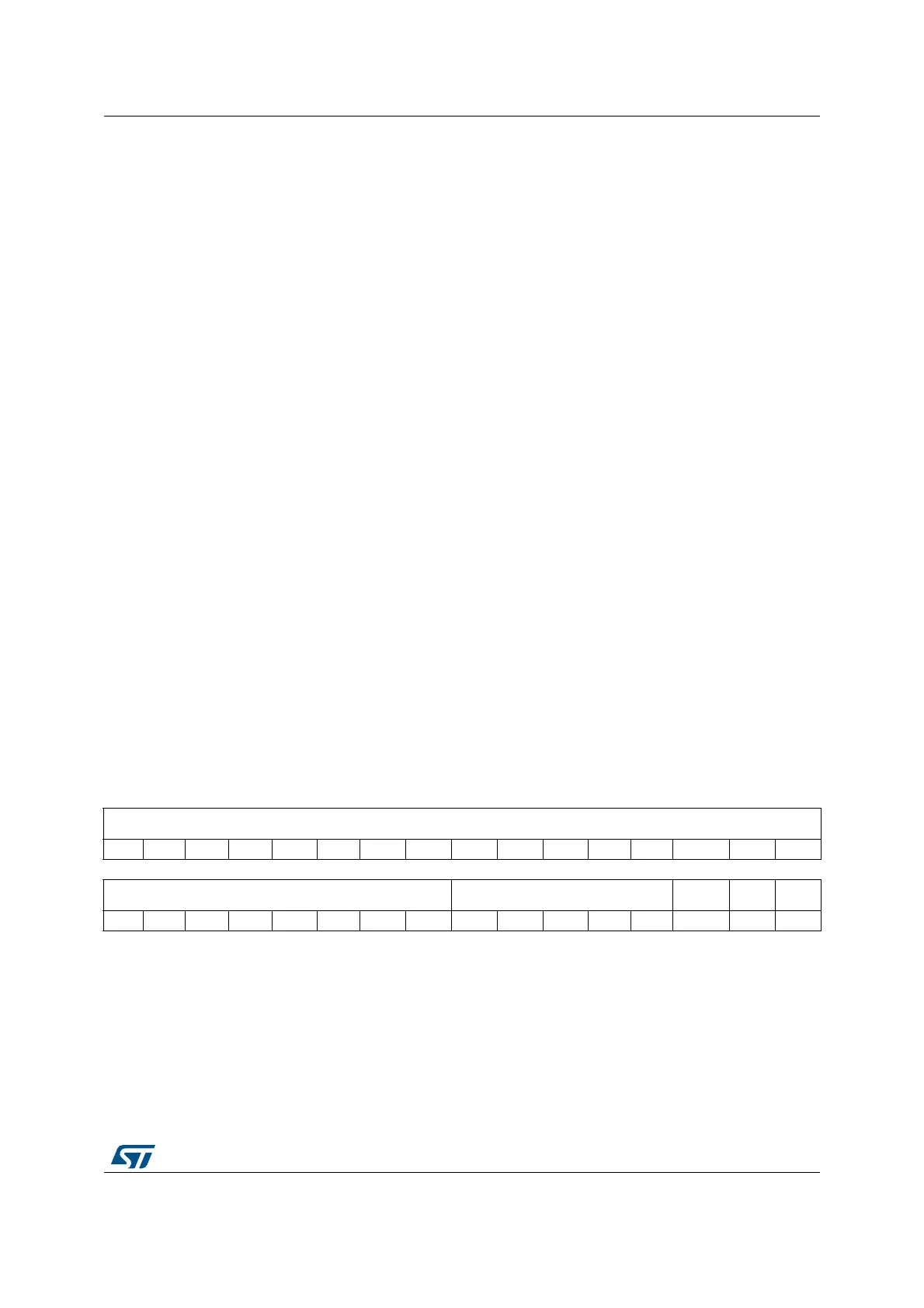
31 30 29 28 27 26 25 24 23 22 21 20 19 18 17 16
OFFSET[23:8]
rw rw rw rw rw rw rw rw rw rw rw rw rw rw rw rw
15 14 13 12 11 10 9 8 7 6 5 4 3 2 1 0
OFFSET[7:0] DTRBS[4:0] Res. Res. Res.
rw rw rw rw rw rw rw rw rw rw rw rw rw

 Loading...


