B1.107 Secure Debug Enable Register
The SDER characteristics are:
Purpose
Controls invasive and non-invasive debug in the Secure EL0 state.
Usage constraints
This register is accessible as follows:
EL0
(NS)
EL0
(S)
EL1
(NS)
EL1
(S)
EL2
EL3
(SCR.NS = 1)
EL3
(SCR.NS = 0)
- - - RW - RW RW
Configurations
SDER is architecturally mapped to AArch64 register SDER32_EL3. See B2.93 Secure Debug
Enable Register, EL3 on page B2-535.
This register is accessible only in Secure state.
If EL3 is using AArch32, write access to SDER is disabled when the CP15SDISABLE2 signal
is asserted HIGH.
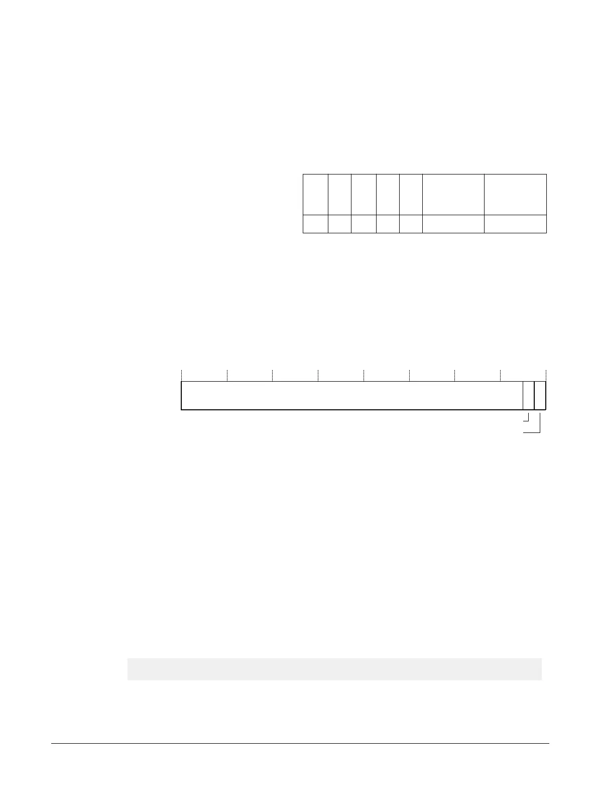
Attributes
SDER is a 32-bit register.
31
0
RES0
SUNIDEN
SUIDEN
12
Figure B1-60 SDER bit assignments
[31:2]
Reserved, RES0.
SUNIDEN, [1]
Secure User Non-invasive Debug Enable. The possible values are:
0 Non-invasive debug not permitted in Secure EL0 state. This is the Warm reset value.
1 Non-invasive debug permitted in Secure EL0 state.
SUIDEN, [0]
Secure User Invasive Debug Enable. The possible values are:
0 Invasive debug not permitted in Secure EL0 state. This is the Warm reset value.
1 Invasive debug permitted in Secure EL0 state.
To access the SDER:
MRC p15,0,<Rt>,c1,c1,1 ; Read SDER into Rt
MCR p15,0,<Rt>,c1,c1,1 ; Write Rt to SDER
Register access is encoded as follows:
B1 AArch32 system registers
B1.107 Secure Debug Enable Register
100236_0100_00_en Copyright © 2015–2017, 2019 Arm Limited or its affiliates. All rights
reserved.
B1-337
Non-Confidential