B2.74 L2 Control Register, EL1
The L2CTLR_EL1 characteristics are:
Purpose
Provides IMPLEMENTATION DEFINED control options for the L2 memory system.
Usage constraints
This register is accessible as follows:
EL0 EL1
(NS)
EL1
(S)
EL2
EL3
(SCR.NS = 1)
EL3
(SCR.NS = 0)
- RW RW RW RW RW
L2CTLR_EL1 is writable. However, all writes to this register are ignored.
Configurations
L2CTLR_EL1 is mapped to the AArch32 L2CTLR register. See B1.92 L2 Control Register
on page B1-303.
There is one L2CTLR_EL1 for the Cortex‑A35 processor.
Attributes
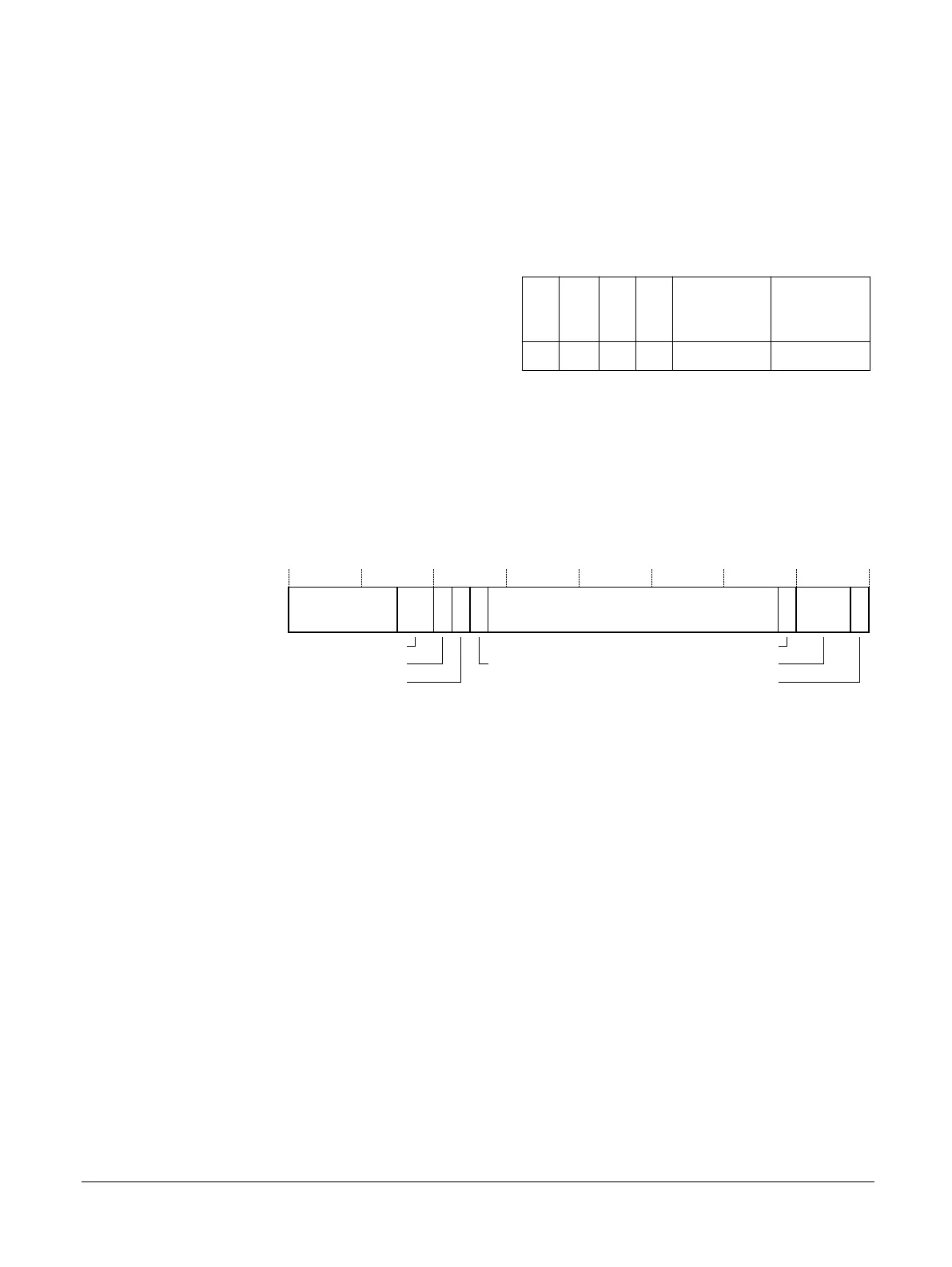
L2CTLR_EL1 is a 32-bit register.
31 0
26 25 24
Reserved
Number of cores
RES0
23 1
L2 Data RAM input latency
22 21 20
Reserved
CPU Cache Protection
SCU- L2 Cache Protection
456
L2 Data RAM output latency
Reserved
Figure B2-46 L2CTLR_EL1 bit assignments
[31:26]
Reserved, RES0.
Number of cores, [25:24]
Number of cores present:
0b00 One core, core 0.
0b01 Two cores, core 0 and core 1.
0b10 Three cores, cores 0 to 2.
0b11 Four cores, cores 0 to 3.
These bits are read-only and the value of this field is set to the number of cores present in the
configuration.
[23]
Reserved, RES0.
CPU Cache Protection, [22]
CPU Cache Protection. Core RAMs are implemented:
0 Without ECC.
1 With ECC.
B2 AArch64 system registers
B2.74 L2 Control Register, EL1
100236_0100_00_en Copyright © 2015–2017, 2019 Arm Limited or its affiliates. All rights
reserved.
B2-489
Non-Confidential