C5.3 Encoding for tag and data in the L1 data cache
The following table shows the format of the Data Cache Tag Read Operation Register and the Data
Cache Data Read Operation Register. The Data Cache Tag Read Operation and the Data Cache Data
Read Operation use the same encoding but the latter includes an additional field to locate the appropriate
doubleword in the cache line.
The set-index range parameter (S) is determined by the following formula:
S = log
2
(size of the data cache in bytes/4).
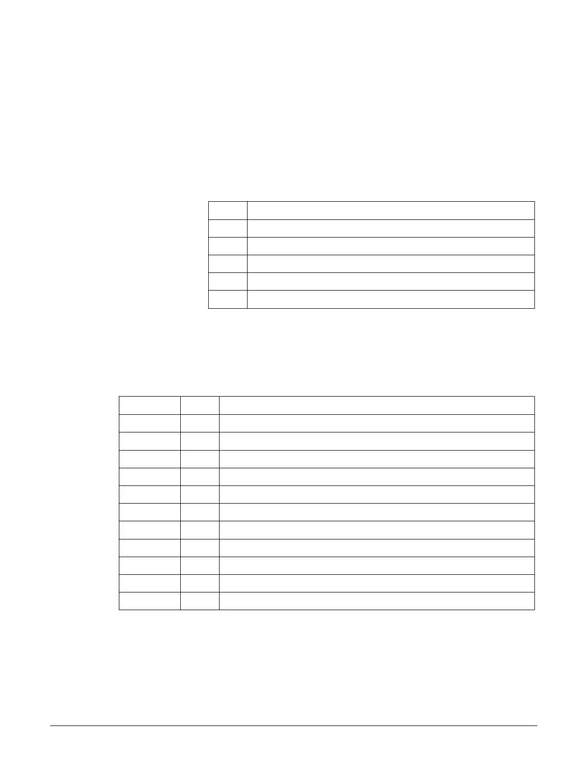
Table C5-5 Data cache tag and data location encoding
Bit field Description
[31:30] Cache way
[29:S] Unused
[S-1:6] Set index
[5:3] Cache doubleword data offset (Data Cache Data Read Operation Register only)
[2:0] Unused, RAZ.
The Data Cache Tag Read Operation returns 64 bits of data in Data Register 0 and Data Register 1. This
includes the tag information, MOESI coherency state, outer attributes, and valid bit, for the selected
cache line. The following table shows the format of the return value. The Cortex‑A35 processor encodes
the 4-bit MOESI coherency state across two fields of Data Register 0 and Data Register 1.
Table C5-6 Data cache tag data format
Register Bit field Description
Data Register 1 [31] Parity bit if ECC is implemented, otherwise RES0.
Data Register 1 [30:29] Partial MOESI State, from tag RAM. See Table C5-7 MOESI state on page C5-611.
Data Register 1 [28] Non-secure state (NS).
Data Register 1 [27:0] Tag Address [39:12].
Data Register 0 [31] Tag Address [11].
Data Register 0 [30:5] Reserved, RES0.
Data Register 0 [4] Parity bit if ECC is implemented, otherwise RES0.
Data Register 0 [3] Dirty copy bit if ECC is implemented, otherwise RES0.
Data Register 0 [2] Outer Allocation Hint.
Data Register 0 [1] Outer Shareability, from Dirty RAM.
Data Register 0 [0] Partial MOESI state, from Dirty RAM. See Table C5-7 MOESI state on page C5-611.
The Data Cache Data Read Operation returns two entries from the cache in Data Register 0 and Data
Register 1 corresponding to the 16-bit aligned offset in the cache line:
Data Register 0 Bits[31:0] data from cache offset+ 0b000.
Data Register 1 Bits[31:0] data from cache offset+ 0b100.
C5 Direct access to internal memory
C5.3 Encoding for tag and data in the L1 data cache
100236_0100_00_en Copyright © 2015–2017, 2019 Arm Limited or its affiliates. All rights
reserved.
C5-610
Non-Confidential