C5.4 Encoding for the main TLB RAM
The Cortex‑A35 processor unified TLB is built from a 2-way set-associative RAM based structure. To
read the individual entries into the data registers, software must write to the TLB Data Read Operation
Register.
The following table shows the format of the TLB Data Read Operation Register.
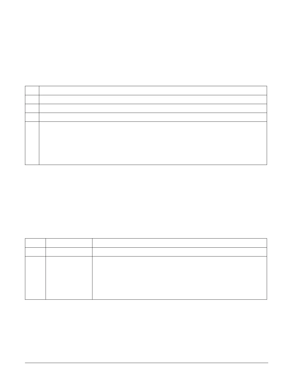
Table C5-8 Location encoding for the TLB Data Read Operation Register
Bits Description
[31] Unused
[30] TLB way
[29:9] Unused
[8:0]
TLB index
0-255 Main TLB RAM
256-287 Walk cache RAM
288-319 IPA cache RAM
320-511 Unused
The TLB Read Data Operation returns the selected entry in Data Register 0-3. The entry uses a 116-bit
encoding when parity is enabled and a 113-bit encoding when parity is disabled.
Data Register 0[31:0] TLB Descriptor[31:0].
Data Register 1[31:0] TLB Descriptor[63:32].
Data Register 2[31:0] TLB Descriptor[95:64].
Data Register 3[20:0] TLB Descriptor[115:96].
The following table shows the data fields in the TLB descriptor.
Table C5-9 Main TLB descriptor data fields
Bits Name Description
[115:113] Parity If CPU cache protection is not implemented, these bits are absent.
[112:111] S2 Level
The stage 2 level that gave this translation:
0b00
No stage 2 translation performed.
0b01
Level 1.
0b10
Level 2.
0b11
Level 3.
C5 Direct access to internal memory
C5.4 Encoding for the main TLB RAM
100236_0100_00_en Copyright © 2015–2017, 2019 Arm Limited or its affiliates. All rights
reserved.
C5-612
Non-Confidential