A.11 AXI interface signals
The AXI protocol supports clock, configuration, and data handling signals when the processor uses this
protocol for the master memory interface.
This interface exists only if the processor is configured to have the AXI interface.
All AXI channels must be balanced with respect to CLKIN and timed relative to ACLKENM.
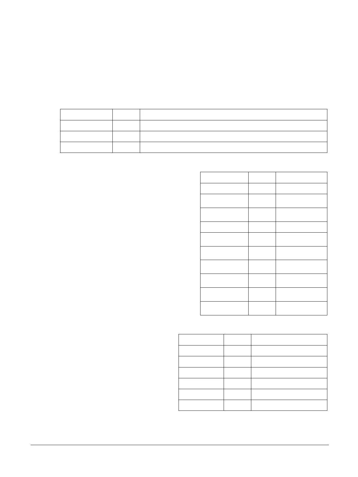
Table A-18 AXI clock and configuration signals
Signal Direction Description
ACLKENM Input AXI Master bus clock enable. See A3.1 Clocks on page A3-50 for more information.
RDMEMATTR[7:0] Output Read request memory attributes.
WRMEMATTR[7:0] Output Write request memory attributes.
Table A-19 AXI write address channel signals
Signal Direction Description
AWADDRM[39:0] Output Write address.
AWBURSTM[1:0] Output
Write burst type.
AWCACHEM[3:0] Output
Write cache type.
AWIDM[4:0] Output Write address ID.
AWLENM[7:0] Output
Write burst length.
AWLOCKM Output
Write lock type.
AWPROTM[2:0] Output
Write protection type.
AWREADYM Input
Write address ready.
AWSIZEM[2:0] Output
Write burst size.
AWVALIDM Output
Write address valid.
Table A-20 AXI write data channel signals
Signal Direction Description
WDATAM[127:0] Output Write data
WIDM[4:0] Output Write data ID
WLASTM Output Write data last transfer indication
WREADYM Input Write data ready
WSTRBM[15:0] Output Write byte-lane strobes
WVALIDM Output Write data valid
A Signal Descriptions
A.11 AXI interface signals
100236_0100_00_en Copyright © 2015–2017, 2019 Arm Limited or its affiliates. All rights
reserved.
Appx-A-862
Non-Confidential