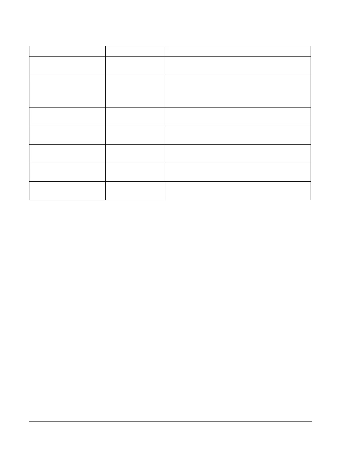
Table A1-2 Implementation options for the processor (continued)
Feature Range of options Notes
L2 cache • Included
• Not included
If it is present, all cores share one L2 cache.
L2 cache size • 128K
• 256K
• 512K
• 1024K
L2 data RAM input latency • 1 cycle
• 2 cycles
L2 data RAM output latency • 2 cycles
• 3 cycles
SCU-L2 cache protection • Included
• Not included
Protects the L2 tag and L2 data RAMs with ECC.
Accelerator Coherency Port (ACP) • Included
• Not included
Part of the SCU-L2. If the processor does not include an L2 cache, it
cannot implement the ACP.
Debug memory map • v8 debug memory map
• v7 debug memory map
Related information
A2.2 Interfaces on page A2-44
A5.5 Invalidating or cleaning a cache on page A5-82
A6.1 About the L1 memory system on page A6-90
A7.1 About the L2 memory system on page A7-98
A5.7 About cache protection on page A5-84
Chapter A12 GIC CPU Interface on page A12-141
C1.6 Debug memory map on page C1-581
C3.1 About the ETM on page C3-596
A1 Introduction
A1.3 Implementation options
100236_0100_00_en Copyright © 2015–2017, 2019 Arm Limited or its affiliates. All rights
reserved.
A1-33
Non-Confidential