Plug/Jack and Wiring Diagrams
Xerox Internal Use Only Phaser 7100 Service Manual 7-57
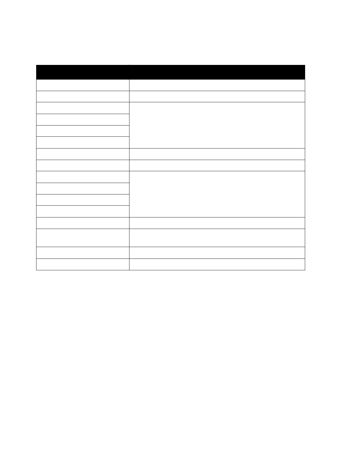
HVPS Signal Lines
Signal Line Name Description
BUR I-Monitor (HVPS2 PWB) The current Monitor signal of the 2nd BUR (Back Up Roller)
TR1 K V-Monitor (HVPS2 PWB) The Voltage Monitor signal of the 1st BTR (K)
DA LD (HVPS2 PWB)
The Output Voltage Level Control signal of the 1st BTR (Y/ M/ C/ K) /
2nd BUR (Back Up Roller)
DA Clock (HVPS2 PWB)
DA DI (HVPS2 PWB)
DA DO (HVPS2 PWB)
BUR Clock (HVPS2 PWB) The Clock signal of the 2nd BUR (Back Up Roller)
Clock 1 (HVPS2 PWB) The Clock signal of the 1st BTR (Y/ M/ C/ K)
DA LD (HVPS1 PWB)
The Output Voltage Level Control signal of the Developer Bias (Y/ M/ C/
K) / BCR (Y/ M/ C/ K)
DA Clock (HVPS1 PWB)
DA DI (HVPS1 PWB)
DA DO (HVPS1 PWB)
Clock A (HVPS1 PWB) The Clock signal of the Developer Bias (Y/ M/ C/ K) AC component
Clock T (HVPS1 PWB) The Clock signal of the Developer Bias (Y/ M/ C/ K) DC component/
BCR (Y/ M/ C/ K)
Deve AC AN The On/ Off Control signal of the Developer Bias (K)
AC YMC AN The On/ Off Control signal of the Developer Bias (Y/ M/ C)
 Loading...