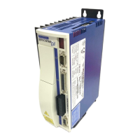
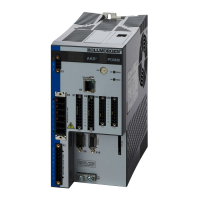
AKD User Guide |
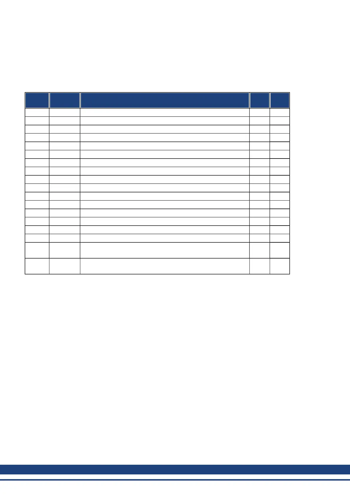
21.4.1 Slave Register
The table below gives the addresses of individual registers in the FPGA memory. The data is provided in little-
endian format, with the ’least significant byte’ occupying the lowest address. A detailed description of all reg-
isters and FPGA memory locations is available in the “EtherCAT Slave Controller” description of the EtherCAT
user organization (www.EtherCAT.org).
Address
Length
(Byte) Description
ZA
ECAT*
ZA
Drive*
0x0120 2 AL Control R/W R/O
0x0130 2 AL Status R/O R/W
0x0134 2 AL Status Code R/O R/W
0x0204 2 Interrupt Enable Register R/O R/W
0x0220 2 AL Event (IRQ Event) R/W R/O
0x0800 8 Sync Manager 0 (Mail Out Control Register) R/W R/O
0x0808 8 Sync Manager 1 (Mail In Control Register) R/W R/O
0x0810 8 Sync Manager 2 (Process data Output Control Register) R/W R/O
0x0818 8 Sync Manager 3 (Process data Input Control Register) R/W R/O
0x0820 8 Sync Manager 4 R/W R/O
0x0828 8 Sync Manager 5 R/W R/O
0x0830 8 Sync Manager 6 R/W R/O
0x0838 8 Sync Manager 7 R/W R/O
0x0840 8 Sync Manager 8 R/W R/O
0x1100 Max. 64 ProOut Buffer (Process data Output, setpoints ECAT) R/W R/O
0x1140 Max. 64 ProIn (Process data Input, act. values ECAT) R/O R/W
0x1800 512 Mail Out Buffer (Object Channel Buffer ECAT,
byte-length is specified in the device description file)
R/W R/O
0x1C00 512 Mail In Buffer (Object Channel Buffer Drive,
byte-length is specified in the device description file)
R/O R/W
* ZA ECAT = Access mode EtherCAT
* ZA Drive = Access mode drive
45 Kollmorgen | December 2010
 Loading...