Parameter Value
Conversion cycle 1 ms (for 4 inputs + 2 outputs); with RTDs Pt/
Ni... 1 s
Resolution Range 0 V...10 V: 12 bits
Range -10 V...+10 V: 12 bits + sign
Range 0 mA...20 mA: 12 bits
Range 4 mA...20 mA: 12 bits
Range RTD (Pt100, PT1000, Ni1000): 0.1 °C
Conversion error of the analog values caused
by non-linearity, adjustment error at factory
and resolution within the normal range
Typ. 0.5 %, max. 1 %
Relationship between input signal and hex
code
Tables Input Ranges Voltage, Current and Dig-
ital Input
Ä
Chapter 1.7.2.2.11.1 “Input
Ranges Voltage, Current and Digital Input”
on page 802 and Input Range Resistor
Ä
Chapter 1.7.2.2.11.2 “Input Range Resistor”
on page 803
Unused inputs Are configured as "unused" (default value)
Overvoltage protection Yes
Technical Data of the Analog Inputs, if used as Digital Inputs
Parameter Value
Number of channels per module Max. 4
Distribution of channels into groups 1 group of 4 channels
Connections of the channels AI0+ to AI3+ Terminals 3.0 to 3.3
Reference potential for the inputs Terminals 1.9, 2.9, 3.9 and 4.9 (ZP)
Indication of the input signals 1 LED per channel
Input signal voltage 24 VDC
Signal 0 -30 V...+5 V
Undefined signal +5 V ... +13 V
Signal 1 +13 V...+30 V
Input current per channel
Input voltage +24 V Typ. 7 mA
Input voltage +5 V Typ. 1.4 mA
Input voltage +15 V Typ. 3.7 mA
Input voltage +30 V < 9 mA
Input resistance ca. 3.5 kW
Technical Data of the Analog Outputs
Parameter Value
Number of channels per module 2
Distribution of channels into groups 1 group for 2 channels
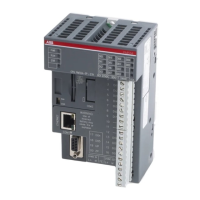
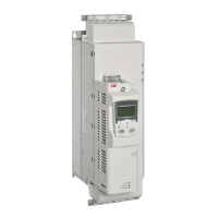
Communication Interface Modules (S500) > CS31
2019/04/17 3ADR010121, 13, en_US 809