IEEE 1149.1 Test Access Port Controller (JTAGC)
MPC5566 Microcontroller Reference Manual, Rev. 2
24-4 Freescale Semiconductor
24.2 External Signal Description
The JTAGC consists of five signals that connect to off-chip development tools and allow access to test
support functions. The JTAGC signals are outlined in the following table:
24.3 Memory Map/Register Definition
This section provides a detailed description of the JTAGC registers accessible through the TAP interface,
including data registers and the instruction register. Individual bit-level descriptions and reset states of
each register are included. These registers are not memory-mapped and can only be accessed through the
TAP.
24.3.1 Instruction Register
The JTAGC uses a 5-bit instruction register as shown in Figure 24-2. The instruction register allows
instructions to be loaded into the module to select the test to be performed or the test data register to be
accessed or both. Instructions are shifted in through TDI while the TAP controller is in the Shift-IR state,
and latched on the falling edge of TCK in the Update-IR state. The latched instruction value can only be
changed in the update-IR and test-logic-reset TAP controller states. Synchronous entry into the
test-logic-reset state results in the IDCODE instruction being loaded on the falling edge of TCK.
Asynchronous entry into the test-logic-reset state results in asynchronous loading of the IDCODE
instruction. During the capture-IR TAP controller state, the instruction shift register is loaded with the
value 0b10101, making this value the register’s read value when the TAP controller is sequenced into the
Shift-IR state.
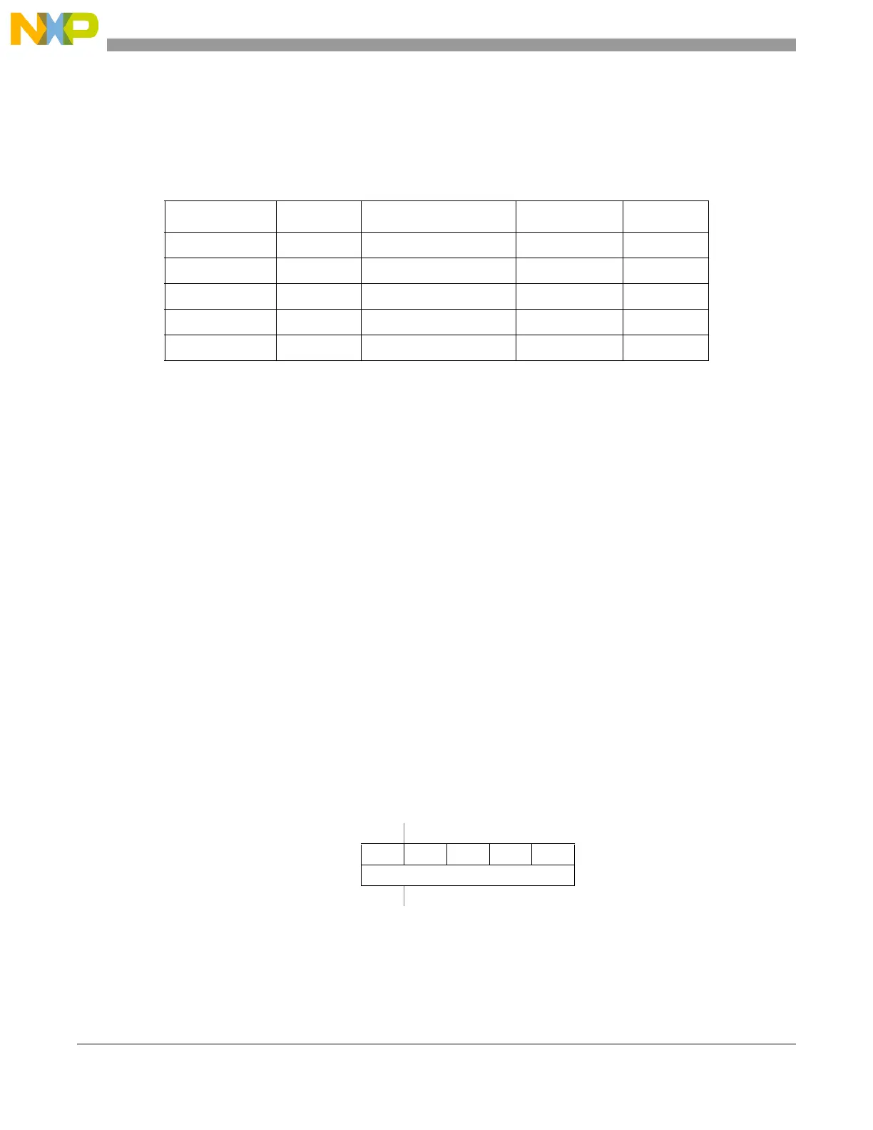
Table 24-1. JTAG Signal Properties
Name I/O Function Reset State Pull
1
1
The pull is not implemented in this module. Pullup/down devices are implemented in the pads.
TCK I Test clock — Down
TDI I Test data in — Up
TDO O Test data out High Z
2
2
TDO output buffer enable is negated when JTAGC is not in the Shift-IR or Shift-DR states. A
weak pulldown can be implemented on TDO.
Down
2
TMS I Test mode select — Up
JCOMP I JTAG compliancy — Down
43210
R1 0 1 01
W Instruction Code
Reset00001
Figure 24-2. 5-Bit Instruction Register

 Loading...


