System Integration Unit (SIU)
MPC5566 Microcontroller Reference Manual, Rev. 2
6-68 Freescale Semiconductor
6.3.1.84 Pad Configuration Registers 122–124 (SIU_PCR122–SIU_PCR124)
The SIU_PCR122–SIU_PCR124 registers control the function, direction, and electrical attributes of
ETPUA[8:10]_ETPUA[20:22]_GPIO[122:124]. ETPUA[20:22] pins operate as output only channels;
ETPUA[8:10] pins can operate as input or output channels.
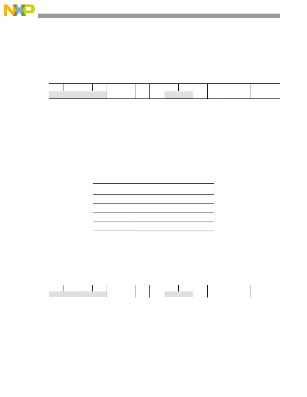
Figure 6-85. ETPUA[8:10]_ETPUA[20:22]_GPIO[122:124]
Pad Configuration Register (SIU_PCR122–SIU_PCR124)
Refer to Table 6-19 for bit field definitions. Table 6-84 lists the PA fields for
ETPUA[8:10]_ETPUA[20:22]_GPIO[122:124].
6.3.1.85 Pad Configuration Register 125 (SIU_PCR125)
The SIU_PCR125 register controls the function, direction, and electrical attributes of
ETPUA[11]_ETPUA[23]_GPIO[125]. Only the output channels of ETPUA[23] are connected. Both the
input and output channels of ETPUA[11] are connected.
Figure 6-86. ETPUA[11]_ETPUA[23]_GPIO[125] Pad Configuration Register (SIU_PCR125)
Address: Base + (0x0134–0x0138) Access: R/W
0 1 2 3 4 5 6 7 8 9 10 11 12 13 14 15
R 0 0 0 0
PA OBE
1
1
The OBE bit must be set to 1 for ETPUA[8:10], or GPIO[122:124] when configured as outputs.
When configured as ETPUA[20], the OBE bit has no effect.
IBE
2
2
The IBE bit must be set to 1 for ETPUA[8:10] or GPIO[122:124] when configured as inputs.
When the pad is configured as an output, set the IBE bit to 1 to show the pin state in the GPDI register.
0 0
ODE HYS SRC WPE WPS
W
RESET: 0 0 0 0 0 0 0 0 0 0 0 0 0 0 1 U
3
3
The weak pullup/down value at reset for ETPUA[8:10] pin is determined by WKPCFG.
Table 6-84. PCR122–PCR124 PA Field Definitions
PA Field Pin Function
0b00 GPIO[122:124]
0b01 ETPUA[8:10]
0b10 ETPUA[20:22]
0b11 ETPUA[8:10]
Address: Base + 0x013A Access: R/W
0 1 2 3 4 5 6 7 8 9 10 11 12 13 14 15
R 0 0 0 0
PA OBE
1
1
The OBE bit must be set to 1 for ETPUA[11] or GPIO[125] when configured as outputs. When configured as ETPUA[23], the
OBE bit has no effect.
IBE
2
2
The IBE bit must be set to 1 for ETPUA[11] or GPIO[125] when configured as inputs. When the pad is configured as an output,
setting the IBE bit to 1 allows the pin state to be reflected in the corresponding GPDI register.
0 0
ODE HYS SRC WPE WPS
W
RESET: 0 0 0 0 0 0 0 0 0 0 0 0 0 0 1 U
3
3
The weak pullup/down selection at reset for the ETPUA[11] pin is determined by the WKPCFG pin.