Enhanced Serial Communication Interface (eSCI)
MPC5566 Microcontroller Reference Manual, Rev. 2
21-4 Freescale Semiconductor
21.3.3 Register Descriptions
This section contains the register descriptions in address order. Each description includes a standard
register diagram with an associated figure number. Details of register bit and field functions follow the
register diagrams, in bit order.
21.3.3.1 eSCI Control Register 1 (ESCIx_CR1)
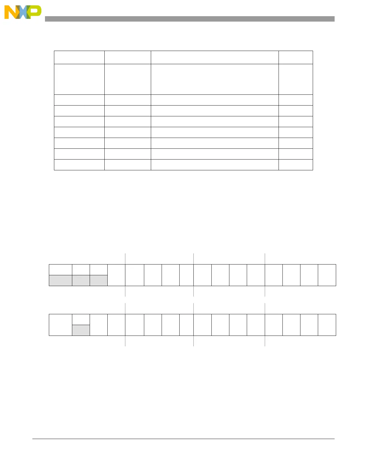
Table 21-2. Module Memory Map
Address Register Name Register Description Bits
Base
0xFFFB_0000 (A)
0xFFFB_4000 (B)
ESCIx_CR1 eSCI control register 1 32
Base + 0x0004 ESCIx_CR2 eSCI control register 2 16
Base + 0x0006 ESCIx_DR eSCI data register 16
Base + 0x0008 ESCIx_SR eSCI status register 32
Base + 0x000C ESCIx_LCR LIN control register 32
Base + 0x0010 ESCIx_LTR LIN transmit register 32
Base + 0x0014 ESCIx_LRR LIN receive register 32
Base + 0x0018 ESCIx_LPR LIN cyclic redundancy check polynomial register 32
Address: Base + 0x0000 Access: R/W
0 1 2 3 4 5 6 7 8 9 101112131415
R0 0 0
SBR
0
SBR
1
SBR
2
SBR
3
SBR
4
SBR
5
SBR
6
SBR
7
SBR
8
SBR
9
SBR
10
SBR
11
SBR
12
W
Reset0 000000000000100
16 17 18 19 20 21 22 23 24 25 26 27 28 29 30 31
R
LOOPS
0
RSRC M WAKE ILT PE PT TIE TCIE RIE ILIE TE RE RWU SBK
W
Reset0 000000000000000
Figure 21-2. eSCI Control Register 1 (ESCIx_CR1)

 Loading...


