Enhanced Queued Analog-to-Digital Converter (eQADC)
MPC5566 Microcontroller Reference Manual, Rev. 2
Freescale Semiconductor 19-39
19.3.3.2 ADC Time Stamp Control Register (ADC_TSCR)
The ADC_TSCR contains a system clock divide factor used in the making of the time base counter clock.
It determines at what frequency the time base counter runs. ADC_TSCR can be accessed by configuration
commands sent to ADC0 or to ADC1. A data write to ADC_TSCR using a configuration command sent
to ADC0 writes to the same memory location as a write using a configuration command sent to ADC1.
NOTE
Simultaneous write accesses from ADC0 and ADC1 to ADC_TSCR are not
allowed.
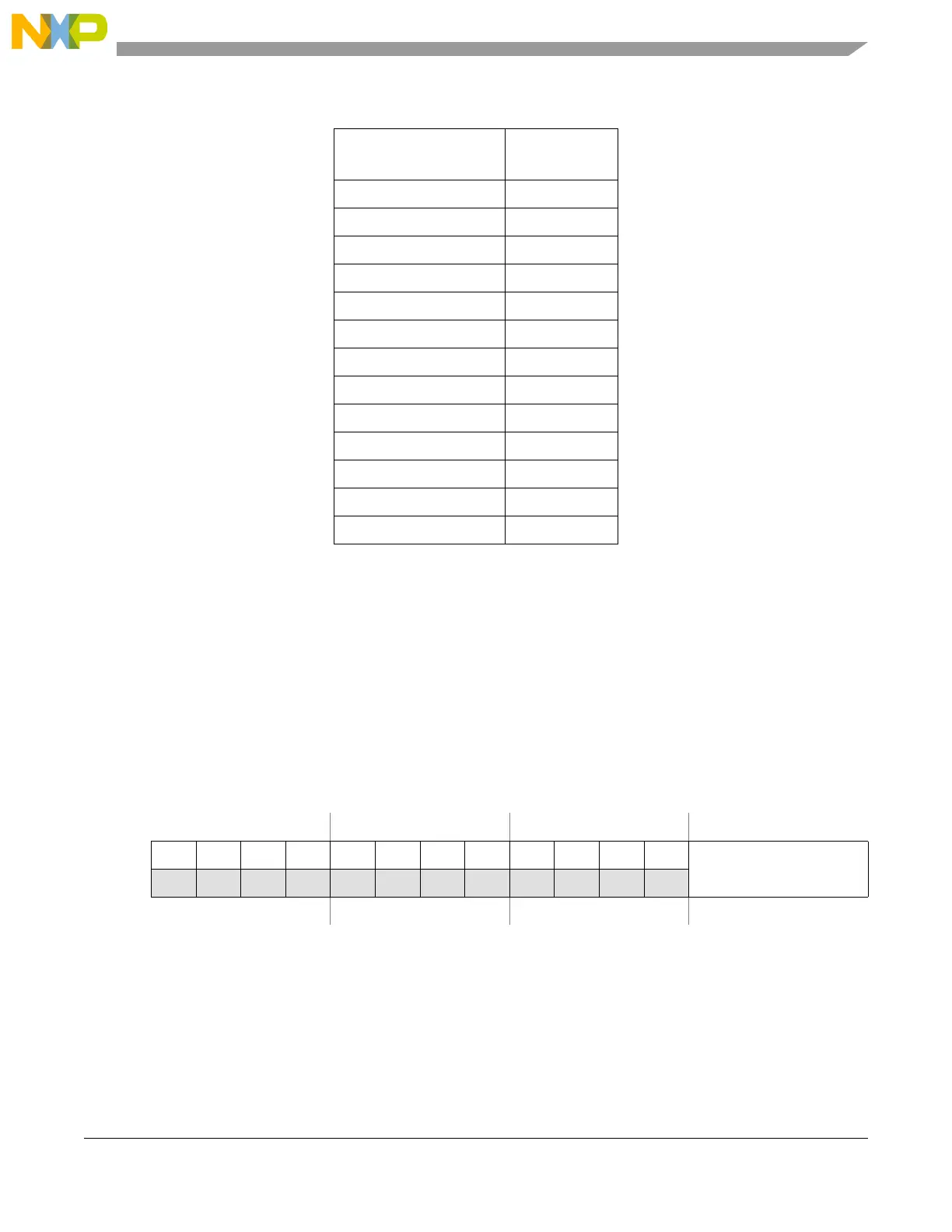
0b10011 40
0b10100 42
0b10101 44
0b10110 46
0b10111 48
0b11000 50
0b11001 52
0b11010 54
0b11011 56
0b11100 58
0b11101 60
0b11110 62
0b11111 64
Address: 0x0002 Access: R/W
0123456789101112131415
R000000000000
TBC_CLK_PS
W
Reset0000000000000000
Figure 19-20. ADC Time Stamp Control Register (ADC_TSCR)
Table 19-28. System Clock Divide Factor for ADC Clock (continued)
ADCn_CLK_PS[0:4]
System Clock
Divide Factor

 Loading...


