System Integration Unit (SIU)
MPC5566 Microcontroller Reference Manual, Rev. 2
Freescale Semiconductor 6-53
Refer to Table 6-19 for bit field definitions. Table 6-61 lists the PA fields for
SOUTA_PCSC[5]_GPIO[95].
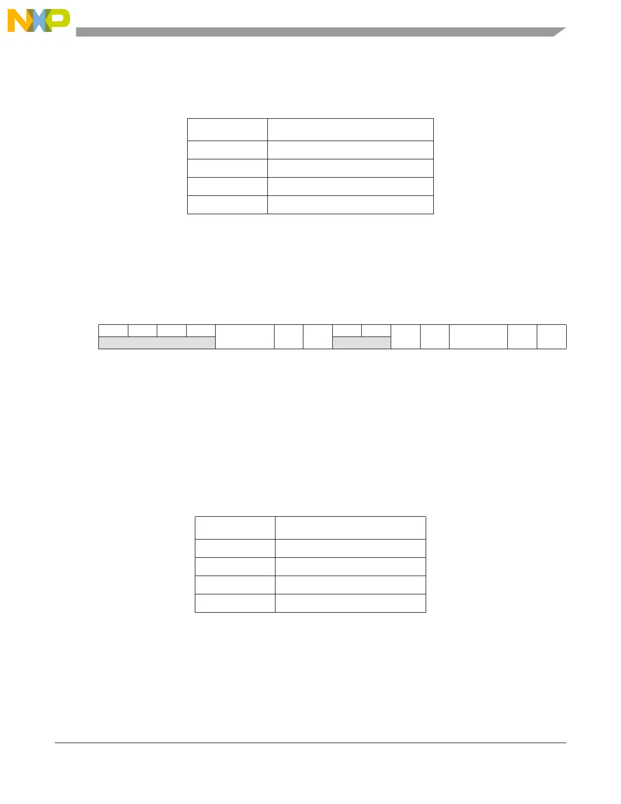
6.3.1.62 Pad Configuration Registers 96 (SIU_PCR96)
The SIU_PCR96 registers control the function, direction, and electrical attributes of
PCSA[0]_PCSD[2]_GPIO[96]. This register allows selection of the PCSA[0], PCSD[2] and GPIO
functions.
Figure 6-63. PCSA[0]_PCSD[2]_GPIO[96] Pad Configuration Register (SIU_PCR96)
Refer to Table 6-19 for bit field definitions. Table 6-62 lists the PA fields for
PCSA[0]_PCSD[2]_GPIO[96].
Table 6-61. PCR95 PA Field Definitions
PA Field Pin Function
0b00 GPIO[95]
0b01 SOUTA
0b10 PCSC[5]
0b11 SOUTA
Address: Base + 0x0100 Access: R/W
0 1 2 3 4 5 6 7 8 9 10 11 12 13 14 15
R 0 0 0 0
PA
1
1
The PCSA[0] function is available on the MPC5566 only.
OBE
2
2
When configured as PSCA[0], set the OBE bit to 1 for master operation, and clear to 0 for slave operation. When configures
as PCSD[2], the OBE bit has no effect. When configured as GPDO, set the OBE bit to 1.
IBE
3
3
When configured as PCSA[0] in slave operation, set the IBE bit to 1. When the pad is configured as an output, set the IBE bit
to 1 to show the pin state in the GPDI register. Clear the IBE bit to 0 to reduce power consumption. When configured as GPDI,
set the IBE bit to 1.
0 0
ODE HYS SRC WPE WPS
W
RESET: 0 0 0 0 0 0 0 0 0 0 0 0 0 0 1 1
Table 6-62. PCR96 PA Field Definitions
PA Field Pin Function
0b00 GPIO[96]
0b01 PCSA[0]
0b10 PCSD[2]
0b11 PCSA[0]