Frequency Modulated Phase Locked Loop and System Clocks (FMPLL)
MPC5566 Microcontroller Reference Manual, Rev. 2
Freescale Semiconductor 11-29
skewed. Finally, the error due to the manufacturing and environment variation alone can cause the
frequency modulation depth error to be greater than 20%.
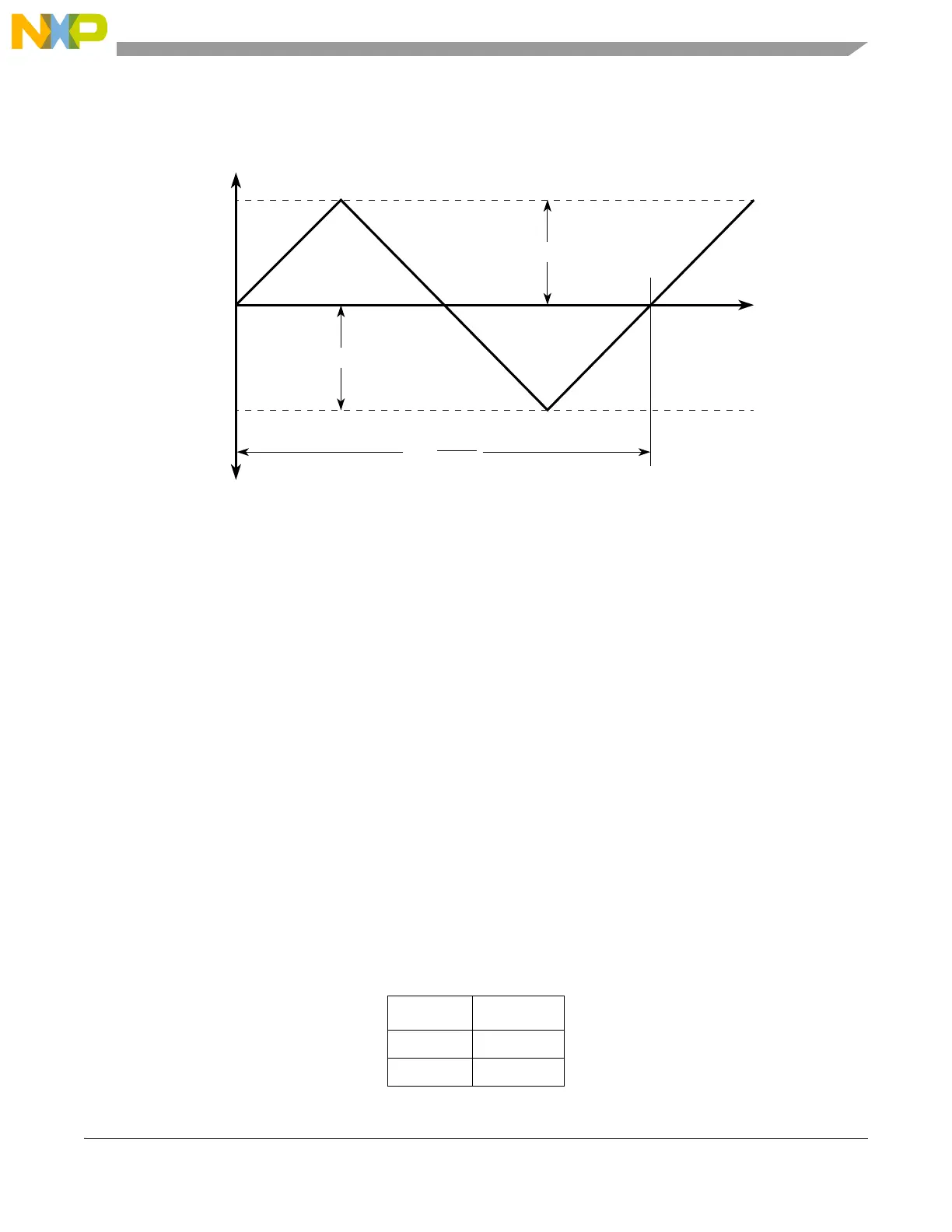
Figure 11-10. Frequency Modulation Waveform
11.4.3.3 FM Calibration Routine
Upon enabling frequency modulation, a new calibration routine is performed. This routine tunes a
reference current into the modulation D/A so that the modulation depth (F
max
and F
min
) remains within
specification.
Entering the FM calibration mode requires you to program SYNCR[EXP]. The EXP is the expected value
of the difference between the reference and feedback counters used in the calibration of the FM equation:
For example, if 80 MHz is the desired final frequency and an 8 MHz crystal is used, the final values of
MFD = 6 and RFD = 0 produces the desired 80 MHz. For a desired frequency modulation with a 1% depth,
then EXP is calculated using P = 1, MFD = 6 and M = 480. Refer to Table 11-10 for a complete list of
values to be used for the variable (M) based on MFD setting. To obtain a percent modulation (P) of 1%,
the EXP field must be set at:
Rounding this value to the closest integer yields 48, which is entered into the EXP field for this example.
Table 11-10. Multiplied Factor Dividers with M Values
MFD M
0–2 960
3–5 640
F
max
= F
sys
+ {1%, 2%}
F
min
= F
sys
– {1%, 2%}
F
mod
= F
ref_crystal
or F
ref_ext
÷ [(PREDIV + 1) × Q] where Q = 40 or 80
F
max
ΔFm
t
F
min
f
Δt =
1
F
mod
ΔFm
EXP
MFD 4+()M× P×()
100
------------------------------------------------------
=
EXP 6 4+()480× 1×()100÷ 48==