Deserial Serial Peripheral Interface (DSPI)
MPC5566 Microcontroller Reference Manual, Rev. 2
20-2 Freescale Semiconductor
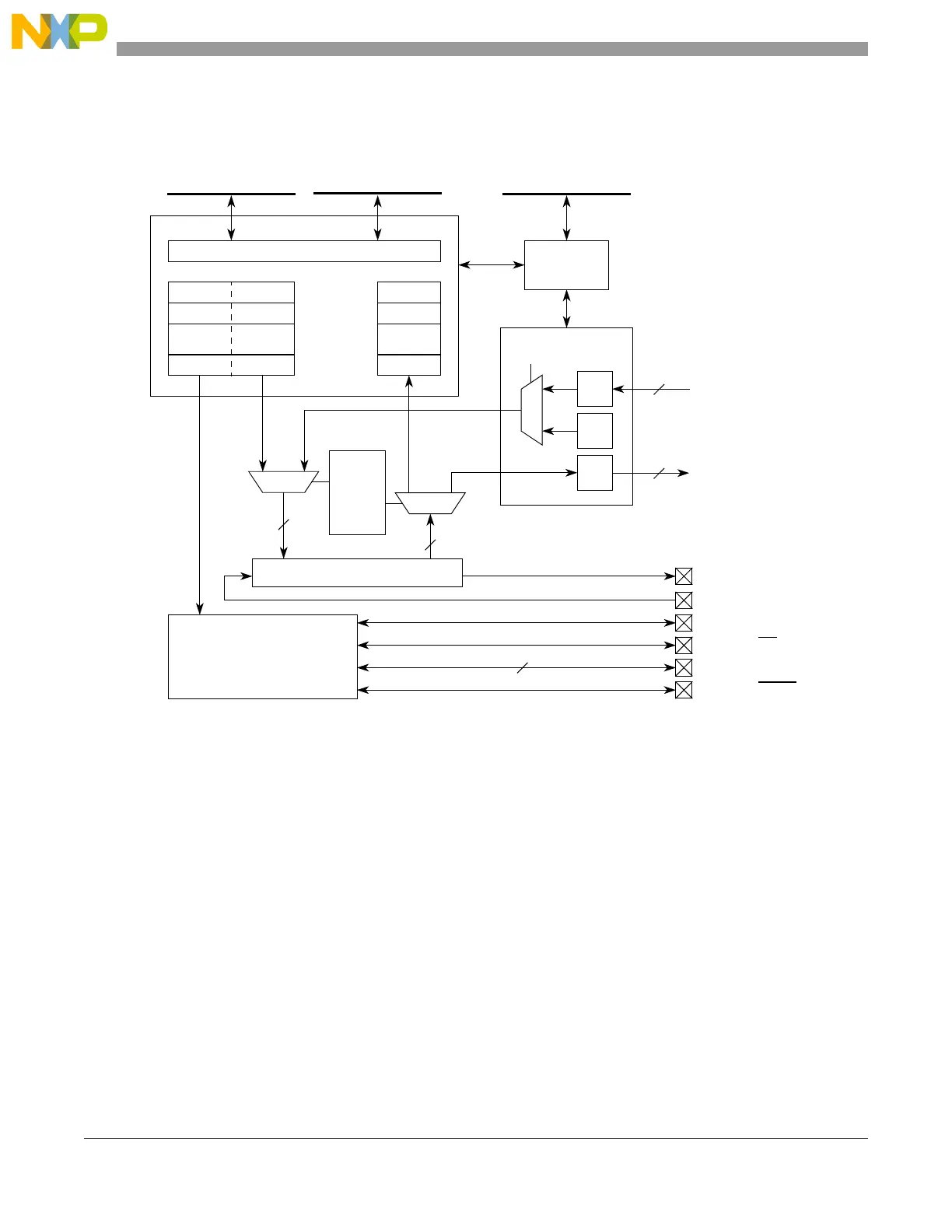
20.1.1 Block Diagram
A block diagram of the DSPI is shown in Figure 20-1.
Figure 20-1. DSPI Block Diagram
20.1.2 Overview
The DSPI supports pin count reduction through serialization and deserialization of eTPU channels, eMIOS
channels, and memory-mapped registers. Incoming serial data may be used to trigger external interrupt
requests through DSPI deserialized output connections to the SIU. The channels and register content are
transmitted using an SPI protocol. There are four identical DSPI modules (DSPI A, DSPI B, DSPI C, and
DSPI D) on the device. The DSPI has three configurations:
• Serial peripheral interface (SPI) configuration where the DSPI operates as an SPI with support for
queues.
• Deserial serial interface (DSI) configuration where the DSPI serializes eTPU and eMIOS output
channels and deserializes the received data by placing the data on the eTPU and eMIOS input
channels and as inputs to the external interrupt request submodule of the SIU.
CMD
DMA and interrupt control
TX FIFO RX FIFO
TX data RX data
16
16
Shift register
SOUTx
SPI
SPI and DSI baud rate,
delay and transfer
control
CSI
priority
logic
TXSS
DSI
DSPI BIU
16
From eTPU
and eMIOS
output channels
16
To eTPU or
eMIOS
input channels
SIU_DISR
SINx
SCKx
PCSx[0]_SS
x
PCSx[1:4]
PCSx[5]_PCSS
x
INTC
eDMA Slave interface
4

 Loading...


