Deserial Serial Peripheral Interface (DSPI)
MPC5566 Microcontroller Reference Manual, Rev. 2
20-52 Freescale Semiconductor
Figure 20-30. CSI Serialization Diagram
The parallel inputs signal states are latched into the DSPIx_SDR on the rising edge of every system clock
and serialized based on the transfer initiation control settings in the DSPIx_DSICR. For more information
on the DSPIx_SDR. SPI frames written to the TX FIFO have priority over DSI data from the DSPIx_SDR
and are transferred at the next frame boundary. A copy of the most recently transferred DSI frame is stored
in the DSPIx_COMPR. The transfer priority logic selects the source of the serialized data and asserts the
chip select signal.
See Section 20.3.2.11, “DSPI DSI Serialization Data Register (DSPIx_SDR).”
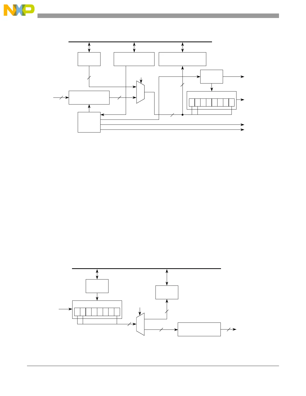
20.4.5.2 CSI Deserialization
The deserialized frames in CSI configuration go into the DSPIx_SDR or the RX FIFO based on the transfer
priority logic. When DSI frames are transferred the returned frames are deserialized and latched into the
DSPIx_DDR. When SPI frames are transferred the returned frames are deserialized and written to the RX
FIFO.
Figure 20-31 shows the CSI deserialization logic.
Figure 20-31. CSI Deserialization Diagram
SOUTx
Parallel
DSI control
register
DSI transmit
comparison register
Clock
logic
0 1 • • • • • 15
Shift register
DSI serialization
data register
Control
logic
SCKx
inputs
PCSx (SPI)
PCSy (DSI)
16
16
16
16
Transfer
Slave bus interface
16
TX FIFO
(P_IN)
priority logic
SIN
Control
logic
0 1 • • • • • 15
Shift register
16
Slave bus interface
Parallel
DSI deserialization
data register
outputs
16
Transfer
priority logic
16
RX FIFO
(P_OUT)
16