Flash Memory
MPC5566 Microcontroller Reference Manual, Rev. 2
Freescale Semiconductor 13-9
13.3.2 Register Descriptions
The flash registers are detailed in the following sections.
13.3.2.1 Module Configuration Register (FLASH_MCR)
A number of module configuration register (FLASH_MCR) bits are protected from a write while another
bit or set of bits are in a specific state. These locks are discussed in relationship to each bit in this section.
Simultaneously writing bits which lock each other out is discussed in Section 13.3.2.1.1, “MCR
Simultaneous Register Writes.” The MCR is always available to be read except when the flash module is
disabled.
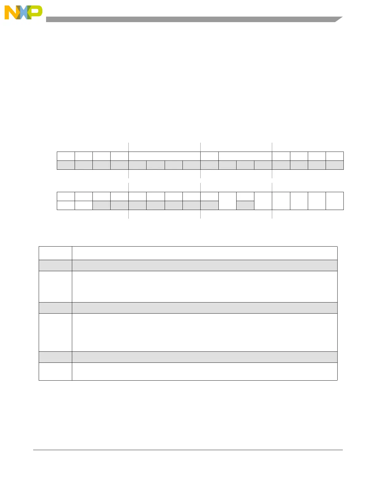
Address: Base (0xC3F8_8000) + 0x0000 Access: R/W
0 1 2 3 4 5 6 7 8 9 10 11 12 13 14 15
R 0 0 0 0 SIZE 0 LAS 0 0 0 MAS
W
Reset0000101111000000
16 17 18 19 20 21 22 23 24 25 26 27 28 29 30 31
R EER RWE 1 1 PEAS DONE PEG 0 0
STOP
0
PGM PSUS ERS ESUS EHV
W
w1c w1c
Reset0011011000000000
Figure 13-4. Module Configuration Register (FLASH_MCR)
Table 13-6. FLASH_MCR Field Descriptions
Field Description
0–3 Reserved.
4–7
SIZE[0:3]
Array space size. Dependent upon the size of the flash module. SIZE is read only.
1011 Total array size is 3 MB
8 Reserved.
9–11
LAS[0:2]
Low address space. Corresponds to the configuration of the low address space. All possible values of LAS
and the configuration to which each value corresponds are shown below. LAS is read only.
110 The LAS value of 110 provides two 16-KB blocks, two 48-KB blocks, and two 64-KB blocks.
12–14 Reserved.
15
MAS
Mid address space size. Corresponds to the configuration of the mid address space. MAS is read only.
0 Two 128-KB blocks are available