MPC5566 Reference Manual Addendum, Rev. 2
Addendum for Revision 2.0
Freescale Semiconductor2
1 Addendum for Revision 2.0
Table 1. MPC5566RM Rev 2.0 addendum
Location Description
Section 12.4.2.7/Page 12-50 Change sentence “The bytes indicated as ‘—’ are not driven during that write cycle” to read “The
bytes indicated as ‘—’ are indeterminate and may be driven during that write cycle.”
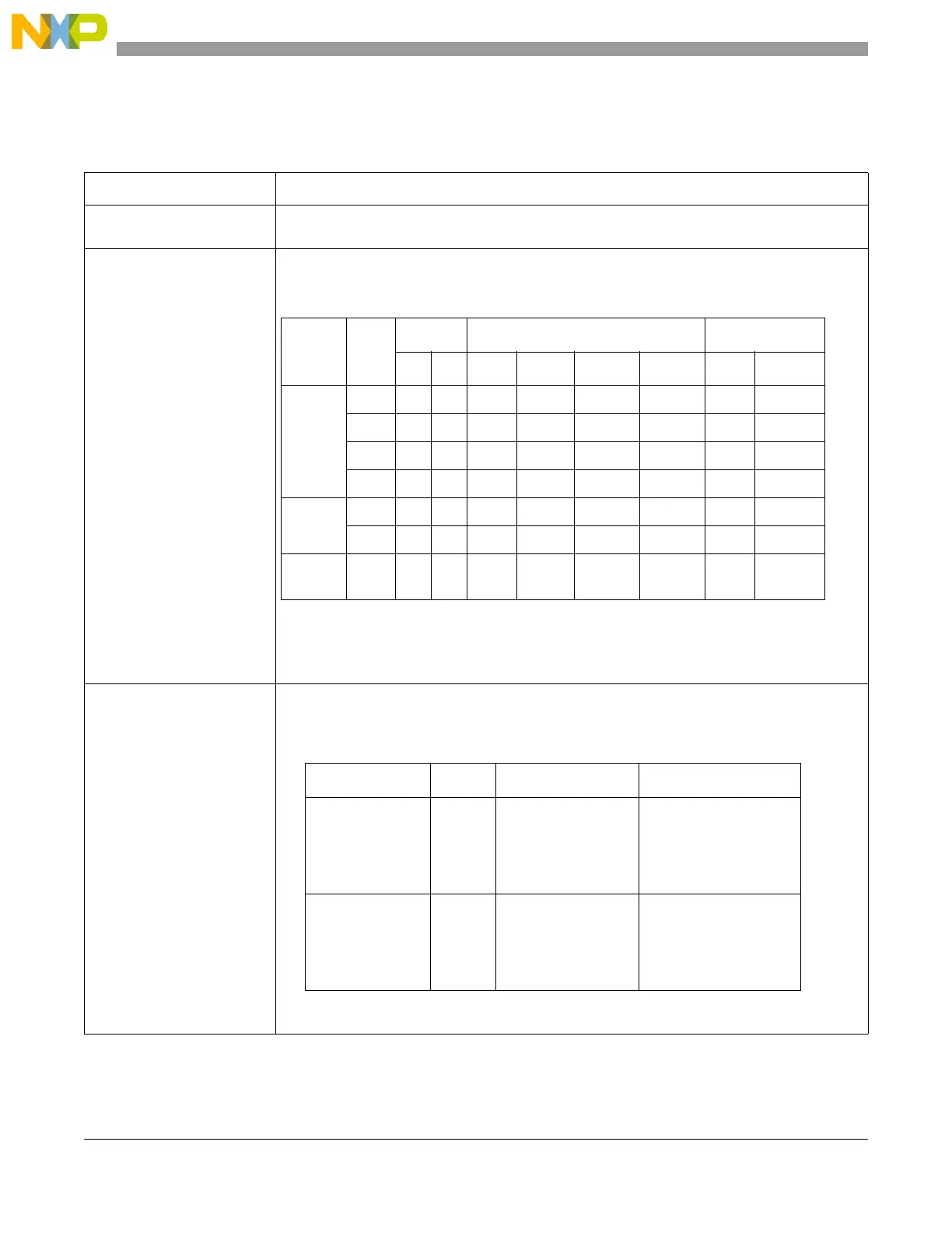
Table 12-21, “Data Bus
Contents for Write
Cycles”/Page 12-50
Replace table with the one below to correct information about data bus contents for write cycles.
Note that only two columns have changed: under “32-Bit Port Size,” columns “D0:D7” and
“D8:D15.”
Table 9-23, “DMA Request
Summary for eDMA”/Page
9-43
Change two rows in the table to correct information about eSCI COMBTX DMA request.
Only the Transmit Data Register Empty and LIN Transmit Data Ready flags drive the DMA
request. The Transmit Complete flag is not used.
Transfer
Size
TSIZ
[0:1]
Address 32-Bit Port Size 16-Bit Port Size
1
1
Also applies when DBM=1 for 16-bit data bus mode.
A30 A31 D0:D7 D8:D15 D16:D23 D24:D31 D0:D7 D8:D15
Byte 01 0 0 OP0 — — — OP0 —
01 0 1 — OP1 — — — OP1
01 1 0 — — OP2 — OP2 —
01 1 1 — — — OP3 — OP3
16-bit 10 0 0 OP0 OP1 — — OP0 OP1
10 1 0 — — OP2 OP3 OP2 OP3
32-bit 00 0 0 OP0 OP1 OP2 OP3 OP0/
OP2
2
2
This case consists of two 16-bit external transactions, the first writing OP0 and OP1,
the second writing OP2 and OP3.
OP1/OP3
DMA Request Channel Source Description
eSCIA_COMBTX 18 ESCIA.SR[TDRE] ||
ESCIA.SR[TC] ||
ESCIA.SR[TXRDY]
eSCIA combined DMA
request of the Transmit
Data Register Empty
and LIN Transmit Data
Ready DMA requests
eSCIB_COMBTX 34 ESCIB.SR[TDRE] ||
ESCIB.SR[TC] ||
ESCIB.SR[TXRDY]
eSCIB combined DMA
request of the Transmit
Data Register Empty
and LIN Transmit Data
Ready DMA requests