Signal Description
MPC5566 Microcontroller Reference Manual, Rev. 2
Freescale Semiconductor 2-17
V
DD33
37
I/O pad pre-driver and level shifter
reference voltage input
PI
3.3 V V
DD33
N/A 3.3 V
A25, C1,
U4, AD9,
AD26
B26, D2, W5,
AE27, AF9
V
SS
Ground P — — V
SSINT
N/A V
SS
A1, A26,
B2, B25,
C3, C24,
D4, D23,
K10, K11,
K12, K13,
L10, L11,
L12, L13,
L14, L15,
L16, M12,
M13, M14,
M15, M16,
N12, N13,
N14, N15,
N16, P12,
P13, P14,
P15, P16,
P17, R12,
R13, R14,
R15, R16,
R17, T11,
T16, T17,
U10, U16,
U17, AC4,
AC23,
AD3,
AD24,
AE2,
AE25,
AF1, AF26
A1, A2, A27,
A28, B1, B2,
B27, B28, C3,
C26, E5, E24,
G7, G22, H8,
H21, L11,
L12, L13,
L14, M12,
M13, M14,
M15, M16,
M17, N14,
N15, N16,
N17, P14,
P15, P16,
P17, R14,
R15, R16,
T13, T16,
T17, U12,
U17, U18,
V11, V18,
AA8, AA21,
AB7, AB22,
AD5, AF3,
AF26, AG1,
AG2, AG27,
AG28, AH1,
AH2, AH27,
AH28, AD24
No Connect
NC
38
No connect N/A N/A N/A N/A N/A N/A
AC22,
AD23
G18, G19,
H17, H18,
AF24, AG25
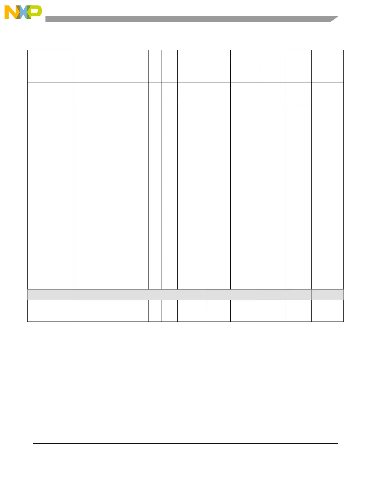
1
For each pin in the table, each line in a Function row is a separate function of the pin. For all MPC5566 I/O pins the selection of primary pin function
or secondary function or GPIO is done in the MPC5566 SIU except where explicitly noted.
2
V
DDE
(fast I/O) and V
DDEH
(slow I/O) power supply inputs are grouped into segments. Each segment of V
DDEH
pins can connect to a separate
3.3–5.0 V (+5% to –10%) power supply input. Each segment of V
DDE
pins can connect to a separate 1.8–3.3 V (±10%) power supply, with the
exception of the V
DDE2
and V
DDE3
segments that are shorted together and must use the same power supply input. This segment is labeled V
DDE2
in the BGA map.
3
The pad type is indicated by one of the abbreviations; F for fast, MH for medium (high voltage), MHA for medium (high voltage) and analog,
SH for slow (high voltage), A for analog. Some pads may have two types, depending on which pad function is selected.
4
The 496 assembly contains the VertiCal base and includes the 416 pins.
5
The Status During Reset pin is sampled after the internal POR is negated. Prior to exiting POR, the signal has a high impedance.
Terminology is O = output, I = input, Up = weak pull up enabled, Down = weak pull down enabled, Low = output driven low, High = output driven
high. A dash on the left side of the slash denotes that both the input and output buffers for the pin are off. A dash on the right side of the slash
denotes that there is no weak pull up/down enabled on the pin. The signal name to the left or right of the slash indicates the pin is enabled.
6
Function after reset of GPI is general purpose input. A dash on the left side of the slash denotes that both the input and output buffers for the pin
are off. A dash on the right side of the slash denotes that there is no weak pull up/down enabled on the pin.
Table 2-1. MPC5566 Signal Properties (continued)
Signal Names Signal Functions
1
P/
A/
G
I/O
Type Voltage
2
Pad
Type
3
Status
416
Package
496
Vertical
Assembly
4
During
Reset
5
After
Reset
6
 Loading...


