TC1796
Peripheral Units (Vol. 2 of 2)
Asynchronous/Synchronous Serial Interface (ASC)
User’s Manual 19-11 V2.0, 2007-07
ASC, V2.0
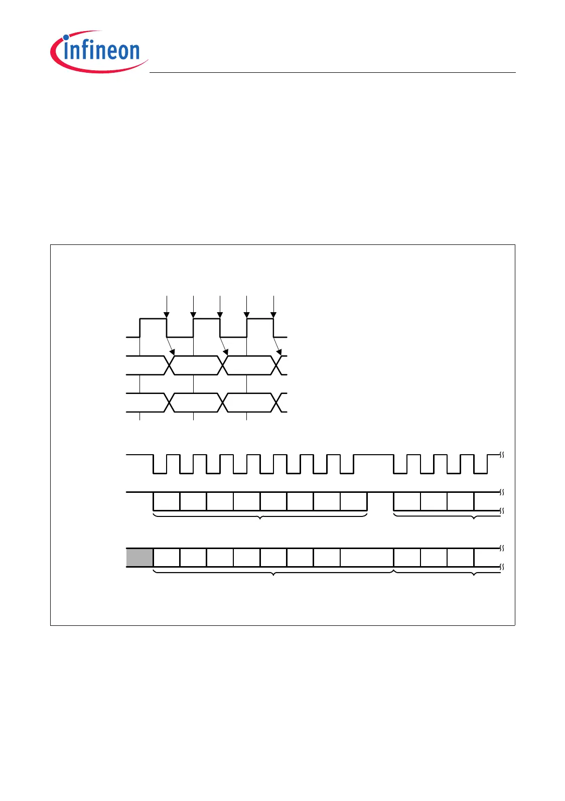
19.1.4.3 Synchronous Timing
Figure 19-7 shows timing diagrams of the ASC Synchronous Mode data reception and
data transmission. In idle state, the shift clock is at high level. With the beginning of a
synchronous transmission of a data byte, the data is shifted out at RXD with the falling
edge of the shift clock. If a data byte is received through RXD, data is latched with the
rising edge of the shift clock.
One shift clock cycle (
f
BR
) delay is inserted between two consecutive receive or transmit
data bytes.
Figure 19-7 ASC Synchronous Mode Waveforms
D0
Valid
Data n+2
Valid
Data n
Valid
Data n+1
Data Bit n+2Data Bit n Data Bit n+1
MCT05768
D1 D2 D3 D4 D5 D6 D7 D0 D1 D2 D3
D0 D1 D2 D3 D4 D5 D6 D7 D0 D1 D2 D3
Receive Data
(RXD)
Transmit Data
(RXD)
Shift Clock
(TXD)
Continuous Transmit Timing
Receive/Transmit Timing
Shift Clock
(TXD)
Receive Data
(RXD)
Shift Latch Shift Latch Shift
1. Byte
1. Byte
2. Byte
2. Byte
Transmit Data
(RXD)

 Loading...