TC1796
System Units (Vol. 1 of 2)
LMB External Bus Unit
User’s Manual 13-74 V2.0, 2007-07
EBU, V2.0
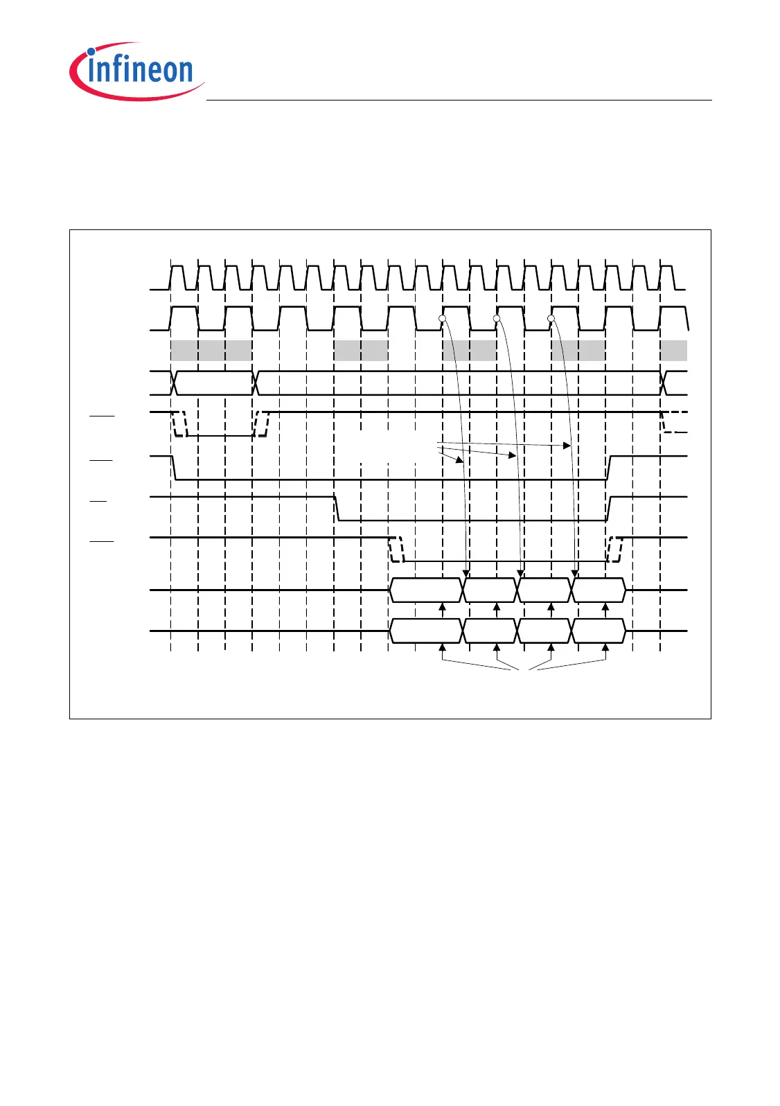
13.9.10 Burst Flash Access Cycle
Figure 13-28 shows an example of a burst read access (burst length of four) with a Burst
Flash device.
Figure 13-28 Burst Flash Read Operation Example (Burst Length of 4)
The Burst Flash access cycle shown in Figure 13-28 is based on the following settings:
• BFCLKO frequency = 1/2 of LMBCLK frequency (EXTCLOCK = 01
B
)
• Address Phase length = 3 LMBCLK cycles (ADDRC = 01
B
)
• Command Delay Phase length = 3 LMBCLK cycles (CMDDELAY = 011
B
)
• Command Phase length = 2 LMBCLK cycles (WAITRDC = 010
B
)
• Burst Phase length = 2 LMBCLK cycles (BURSTC = 010
B
)
• Recovery Phase length = 2 LMBCLK cycles (RDRECOVC = 010
B
)
• Burst Length = 4 (FETBLENn = 010
B
)
• Bus Width = 16-bit (PORTW = 01
B
) or 32-bit (PORTW = 10
B
)
Note that the cycle multiplier control capability is disabled in the example
(MULTMAP = 00
H
).
AP1 AP2 AP3 CPi1 CPi2 BP1 BP2
new
AP1
BP1 BP2CDi1 CDi2 CDi3 BP1 BP2 BP1 BP2 RP1 RP2
LMBCLK
A[23:0]
Addr
MCT05739
CSx
RD
Data in
Addr. + 0
BFCLKO
ADV
Data in
Addr. + 4
Data in
Addr. + 8
Data in
Addr. + 12
D[31:0]
(32-bit)
Data in
Addr. + 0
Data in
Addr. + 2
Data in
Addr. + 4
Data in
Addr. + 8
BAA
D[15:0]
(16-bit)
Next data
issued by Flash
Data latched in EBU

 Loading...