TC1796
Peripheral Units (Vol. 2 of 2)
Micro Second Channel (MSC)
User’s Manual 21-25 V2.0, 2007-07
MSC, V2.0
21.1.3.4 Baud Rate
The baud rate of the upstream channel is derived from the MSC module clock f
MSC
.
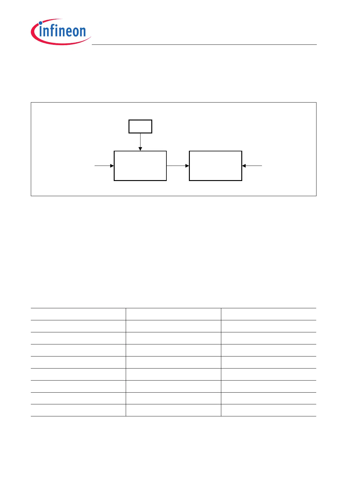
Figure 21-17 shows the configuration of the upstream channel clock circuitry.
Figure 21-17 Upstream Channel Clock Circuitry
The serial data input SI is evaluated with the baud rate clock f
BR
in the middle of each bit
cell, and latched in case of a data bit. The baud rate clock f
BR
is derived from f
MSC
by a
programmable clock divider. The frequency of f
BR
determines the width of a received bit
cell and therefore the baud rate for the receive data. The content of bit field USR.URR
selects the baud rate according Table 21-6. The resulting baud rate formula is:
(21.2)
Note: With the USR.URR = 000
B
the upstream channel is disabled and data reception
is not possible.
Table 21-6 Upstream Channel Divide Factor DF Selection & Baud Rate
USR.URR Divide Factor DF Baud Rate
000
B
reception disabled –
001
B
4 f
MSC
/4
010
B
8 f
MSC
/8
010
B
16 f
MSC
/16
100
B
32 f
MSC
/32
101
B
64 f
MSC
/64
110
B
128 f
MSC
/128
111
B
256 f
MSC
/256
MCA05811_mod
Programmable
Clock
Divider
f
BR
f
MSC
URR
USR
Receive Buffer SI
Baud rate
MSC Upstream Channel
f
MSC
DF
-----------=

 Loading...