TC1796
System Units (Vol. 1 of 2)
LMB External Bus Unit
User’s Manual 13-5 V2.0, 2007-07
EBU, V2.0
The third read/write control line, MR/W, can be used to connect external devices directly
to an asynchronous Motorola-style bus interface. MR/W goes to a low level during a write
cycle, and will stay at high during a read cycle.
13.2.6 Address Valid, ADV
The address valid signal, ADV, validates the address lines A[23:0]. It can be used to latch
these addresses externally.
13.2.7 Byte Controls, BC[3:0]
The byte control signals BC[3:0] select the appropriate byte lanes of the data bus for both
read and write accesses. Table 13-2 shows the activation on access to a 32-bit, 16-bit
or 8-bit external device. Please note that this scheme supports little-endian devices.
The BCx lines are not activated during Burst Mode cycles.
Signals BCx can be programmed for different timing. The available modes cover a wide
range of external devices, such as RAM with separate byte write-enable signals, and
RAM with separate byte chip select signals. This allows external devices to connect
without any external “glue” logic.
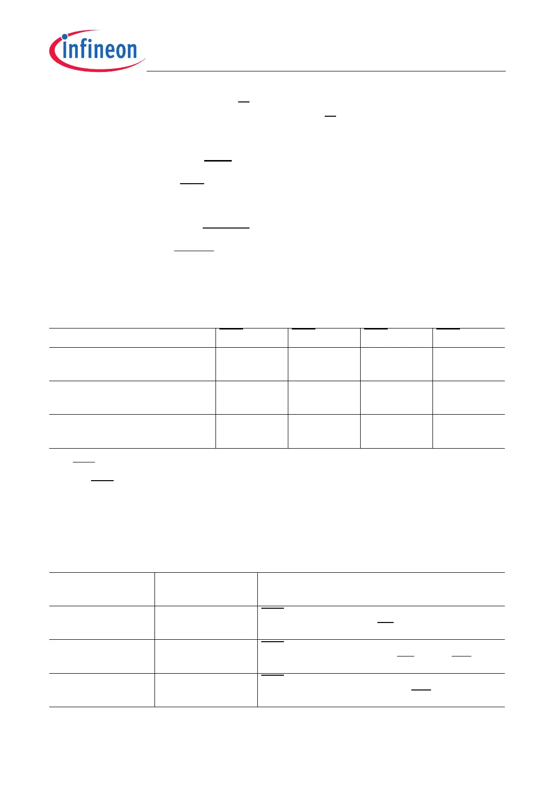
Table 13-2 Byte Control Pin Usage
Width of External Device BC3 BC2 BC1 BC0
32-bit device
with byte write capability
D[31:24] D[23:16] D[15:8] D[7:0]
16-bit device
with byte write capability
inactive
(high)
inactive
(high)
D[15:8] D[7:0]
8-bit device inactive
(high)
inactive
(high)
inactive
(high)
D[7:0]
Table 13-3 Byte Control Signal Timing Options
Mode EBU_BUSCONx.
BCGEN
Description
Chip Select Mode 00
B
BCx signals have the same timing as the
generated chip select CS.
Control Mode 01
B
BCx signals have the same timing as the
generated control signals RD or RD/WR.
Write Enable Mode 10
B
BCx signals have the same timing as the
generated control signal RD/WR.

 Loading...