TC1796
System Units (Vol. 1 of 2)
General Purpose I/O Ports and Peripheral I/O Lines
User’s Manual 10-82 V2.0, 2007-07
Ports, V2.0
10.13.2 Port 10 Registers
The following registers are available on Port 10:
Note: The complete address map of Port 10 is described in Table 18-19 on Page 18-32
of this TC1796 System Units (Vol. 1 of 2) User’s Manual.
Note: Bit field HWCFG in register RST_SR contains the latched logic levels of the
Port 10 inputs that were detected at the last low-to-high transition of HDRST.
Register P10_IN makes it possible to read the actual logic levels of the Port 10
inputs.
10.13.2.1 Port 10 Input Register
The basic P10_IN register functionality is described on Page 10-17. Port lines P10.[15:4]
are not available. Therefore, the P10_IN bits P[3:0] are always read as 0.
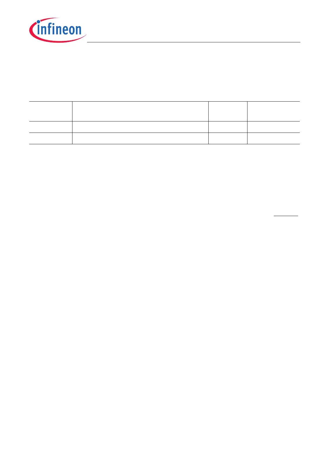
Table 10-27 Port 10 Registers
Register
Short Name
Register Long Name Offset
Address
1)
1) The absolute addresses are calculated by adding the offset address to the module base address (see
Table 10-2)
Description
see
P10_IN Port 10 Input Register 0024
H
Page 10-82
2)
2) This register is listed here in the Port 10 section because it differs from the general port register description
given in Section 10.2.
RST_SR Reset Status Register – Page 4-3

 Loading...